


jcx
-
Posts
34 -
Joined
-
Last visited
Content Type
Profiles
Forums
Events
Posts posted by jcx
-
-
I like knowing more about the part - the later IXTP01N100 datasheet has capacitance curves - while the CCS datasheets are missing these specs
so I would definitely roll my own CCS with the IXTP01N100
just tried hacking the IXYS 10m90 SPICE model into LTspice - I get 100 pF Cds @ 200 Vds in sim - an order of magnitude worse than the IXTP01N100D mosfet datasheet
have any of you measured these parts dynamically? - I doubt they're really that bad but I believe the mosfet datasheet a lot more
-
dual mono isn't "overkill" with Class A balanced output - it is closer to "not even wrong"
Class A balanced output draws constant current from the PS - there isn't any interaction between channels via the PS if they are both ~ ccs loads irrespective of audio signal in either channel
even in clipping the most common situation will be Voltage clipping - low frequency audio signals don't draw any appreciable current drivng ES, are the most common large amplitude signals
-
odd subject for the KGSSHV thread
is there really any issue with power sequence in the BH - the ss ccs loads always limit the output tube current
-
I'm aways curious about how solid teflon machined parts, especially any press fits, are expected to work for decades - has teflon creep, stress relaxation been taken into account?
machining vs application temp can be a mechanical dimension tolerance issue too with a (crystal transition?) thermal expansion coefficient peak occurring around room temp - close to 1% volume change in range from 60 - 90 F
http://www.rjchase.c...fe_handbook.pdf
I would expect chassis mounting pretty much requires spring washers with flat washer - since I certainly have >60-90 F range in my apt over the course of a year
solid polystyrene stock is also available - different problems, still great electrical properties
-
-
I think the SRPP should be viewed as a modulated CCS like Pass Aleph http://www.passdiy.c...df/zen-ver2.pdf - the 50% split of AC current seems likely to optimize efficiency of bias current/power dissapation with little danger of destabilizing gain swings that the higher modulation levels of the mu follower extreme
Pass shows enhancment mode power fet with bjt regulator and AC coupled modulation - with depeltion mode power fet and tapped resistor string the circuit is a lot simpler
I tried talking about these ideas in the T2 thread when the good Doctor asked/speculated about alternatives
-
A few questions... Is CTR important? Is it better to let the base of the transistor float, or tie it to the opto? Looks like a good strategy for a 'stat amp...
the gate drive opto isolators provide floating V ~8V from a string of photodiodes that you can series with the enhancement fet gate to get "depletion mode" equivalent - but the floating V source can provide very little current, < 10 uA - quite enough for mosfet gate drive though
some C in parallel with the photodiodes assures enough charge capacity to soak up Crss slewing current - possibly a "gate stopper" R would assure RF stability
http://www.irf.com/product-info/datasheets/data/pvi5013r.pdf
noise and V ref stablity over temp, LED life are possible issues - depending on mosfet gate threshold V you should have enough V headroom to put a jfet or LM334 ccs in series with the mosfet source - pretty much eliminating concerns about the gate V quality that you would have if you simply used a source series R to set the current
-
-
looking in PAIR Nelson has paid up his maintance fees on 5,376899, 17 years from 12/27/94 issue date still gives him the rest of this year
but from his various statements it seems unlikely that a "public domain" headphone amp project would be a problem for him
-
I think the tl431 would be best avoided - as an amplified band gap reference working down to low currents it is inherently noisy - and as a feedback loop amplifier it is poorly characterized
band gap reference noise can be OK for audio when you insert a lowpass filter after but the required low corner frequency complicates startup dynamics
http://www.analog.com/library/analogDialogue/archives/32-1/xfet.html - precision instrumentation designers often look at the .1-10 Hz noise number - audio really doesn't care given low frequency insensitivity of hearing
http://cds.linear.com/docs/LT%20Magazine/LTMag-V19N1-03-References-BrendanWhelan.pdf
buried Zener LM329 is still available and is probably the cheapest of the buried Zener devices
with the heavy output C the feedback amplifier inside the regulator probably ends up with the output Cload determining the dominant pole compensation
for T2 use "reasonable" 1/f, drift, tempco could be adequate - I'd look for the 1 KHz S/N - don't forget to divide by the Vref value
-
I'm still guessing that U7,8 op amps outputs common mode V is unconstrained and its possible the circuit "works" with one of them saturated at a rail
I would just use one differential integrator and turn the 2nd op amp into a gnd referenced inverter of the 1st's output
then a resistor from each op amp out to the 2 cascode Q would give offset currents that are symmetric about a common bias value
-
does the offset op amp circuit need a common-mode servo/control?
at a 1st glance it looks to me like it would be perfectly happy with one op amp integrating to a rail on one side with the other then working "single ended" to servo the offset
-
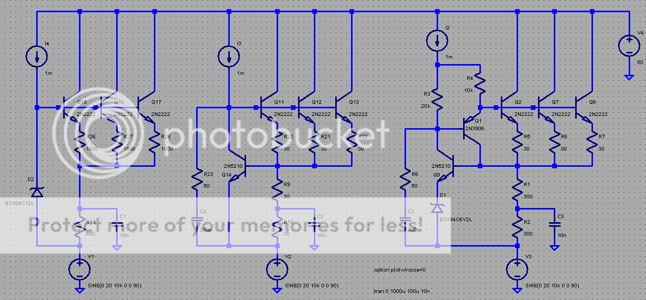
um, I said the 1 mA spice ccs ~= the T2 cascaded pnp ccs - I'm trying to show the circuit mods fit in the existing T2 output ccs topology
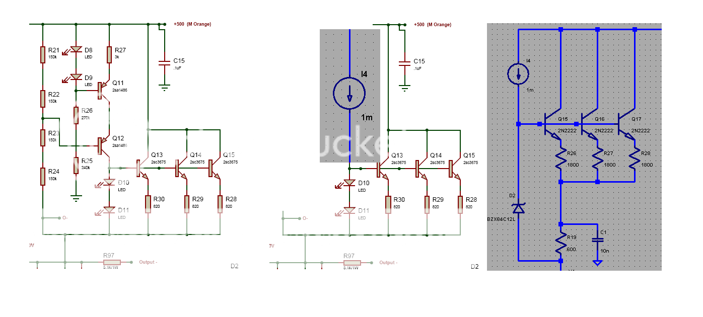
the push-pull operation of my 1st circuit seems to be one way to increase slew rate using the same number of parts as the existing T2 ccs
-
the Pass A40 might be considered an ancestor of SS modulated push-pull Class A bias, Pass still uses a variant of the modulated current source in his recent Class A amps
I previously showed splitting the "sense" R to get push-pull output with a fet ccs
this can easly be done with the T2 Vref+bjt ccs too
obviously the sims are just circuit sketches - and the V and Cloads are scaled down/upto keep currents ~ the same as T2 output ccs - the Q models are just what LTspice include
common to the T2 output ccs circuit: triple pass Q with 2n2222 models are really bad approximations of the 2sc3675, cascaded pnp ccs is approximated with the spice ccs
in the 1st sim I show a circuit with no more parts than already exist in the T2 output ccs but theoretically gives 2x output current swing - which could double slew rate for the same quiescent bias current setting (I assummed ~10 mA output bias)
the 1st circuit uses a higher Vref 12 V Zener to get some added "loop gain" (relax, its all local degeneration) - since the circuit modulates the bjt current we can expect distortions from Vbe/Ic and Vref bias varying when the pass bjt base currents change
does the 2x gain, doubled slew rate compensate for the now varying ccs Q Vbe, Ib caused errors? - someone would have to build and measure
the next two circuits use the same triple pass Q but use local loop feedback to control the current and may be seen as derived from the "ring of two" bjt feedback ccs
the feedback Q Vbe is the Vref for the circuit in the 2nd push-pull current source
the third uses Hawksford/Baxandall "Super Pair" to give cascode like cancellation of Zcb, and the extra current gain reduces the feedback Q/Vref bias variation gain - the feedforward increases the "Q" and the circuit will have RF problems - but so does the Cascode that is AC referred to the "control" Q emitter - I believe it can be tamed with Zobel like RF damping that has little effect on the performance improvements at audio frequency
I also added Zener Vref in the feedback Q emitter to allow higher current sensing R values so the feedforward is more effective (although the improvement may just be from the added current gain)
I probe the load C, Vsource currents and look at fft plot to get an idea of the circuit topology effects - all have falling harmonic level with increasing order - the current control feedback versions I(Cload)distortions start ~ 40 dB lower than the 1st circuit, Vsource current are what an "ideally" controlled output tube would have to do to make the V distortion =0 at this point, I(Vsource)is lowest with 3rd circuit
the third "kitchen sink" circuit's higher frequency harmonics fall faster with increasing order so some of Hawksford's "slope impedance distortion reduction" appears to be taking place in the sim
-
...I just don't see any way to improve on the
design. Maybe ways to make it a bit cheaper
and easier to build, but doing anything
to increase the slew rate, or further lower
the distortion does not seem to be possible.
ghosh, thank you Buddha Gilmore for choosing the path of a bodhisattva when as an Enlightened One you can just step off of the wheel...
as someone liking beer and barbeque too much to sit around staring at a single grain of rice all day long I would try some tricks from Hawksford's Slope Distortion Reduction paper on the ccs, along with the current modulation trick I've already shown
but what I'd really do is add lots of loop gain...
-
xfmr manufacturer's idea of "reasonable" Bmax and definition of "saturation" can be a little scary - I've seen pri excitation currrent jump 5-10x for a 20% high line V compliance test
if you're specing custom try to get them to use the next larger core size
-
I don't do "how does X op amp sound" but technically speaking the ADA4898 is something new and uniquely suited to the objective, technical demands of I/V conversion
it can tolerate 4 mV of I/V DAC switching "glitch" spikes on the input without moving the input stage into nonlinear operation (-120 dB incremental linearity change with 4mV diff input)
this isn't obvious from the data sheet but Scott Wurcer and another AD insider I know revealed that it uses the Gilbert Multi-Tanh linearization scheme - with a patented noise reducing twist
it also is faster, has rather higher output current capability than the NE5534 it replaces in this circuit - which reduces feeedthu with the highly desirable feedback C establishing the 1st pole of your anti-alias filter
the feedback C at the I/V op amp cuts slew rate and glitch feedthru to following circuits - if the I/V op amp is fast enough and has enough current capacity to prevent the glitches from simply "shooting" thru the C at high frequency
you can see that the circuit designers were concerned about the switching glitches causing nonlinearity with the conventional bjt diff pair input of the NE5534 by the inclusion of the input filter to the I/V chip
I would try the ADA4898 with feedback C and bias the output 2-5x the PCM-63 output current, skipping the input filter
-
I thought that opening the design to using SS output means major differences in parasitic C, gm, gain linearity, operating points vs the output tube and slow, low gain, bjt ccs are inevitable and that you might be open to examining the engineering principles behind the device choices for our benefit
if IXYS Vertical Mosfet are ruled out for gm nonlinearity or Rds the choice between Semisouth JFETs can be determined by how you choose to weight several differences - I don't think 3-5 V difference in Vgs bais point is as important as ~4x higher parasitic (and nonlinear) C
particularly when the larger parasitic C values becomes similar to or even more than the ES headphone load C
with the T2 "Rush Cascode" gain stage and using ~ same parasitic C device for the ccs you have to drive ~ 2xCrss + 1xCds for ~150pF with the higher C parts, estimating from the graphs
you don't get the ordinary Cascode's small signal cancellation of Cds when the 2sj79 gm is larger than the JFET's gm - although its hard to make a very good guess at the JFET 10 mA gm from the datasheet curves
there is even a fraction, possibly substantial, additional Cds from the ccs JFET depending on gm and current set R values
the ccs certainly doesn't look as "elegant" with the needed positive bias with the lower parasitic C sje170r555 part - but the solutions can be cheap/no more complicated than the preexisting T2 circuitry for the same function
if you really need to replicate the T2 operating points to better than any differing manufacturer's tube's variations then you can add degeneration R to the cascode JFET source to match the much lower tube gm; for V operating point just change the Zener V
as to how substituting any of the JFET, Mosfet options would effect the "sweetness" of the T2's sound I certainly would guess the doubling the load with added parasitic C and doubling operating current to compensate may have at least some effect
-
...The normally on part cannot be used as the gain stage because that messes with all the
bias stuff elsewhere. The 2sj79 would not be able to drive it.
I understand cascode drive, you have nearly 50 Vds on the 2sj79 so I don't see how operating points change with even 10 V difference in common gate pass device Vgs
"normally on, normally off" is just a gate drive V offset and the pass Q Vgs, 2sj79 Drain V has little effect anywhere else in the circuit
my ccs comments are a little confused - by "SRPP" I was thinking of modulated current source like the sim (just used parts already in Ltspice, think of it as "impedance scaled")
by splitting the "current sense" R and adjusting ratio for equal current swing with jfet gm you nearly double current swing vs a constant current source - even easier with bjt device since you can usually ignore the Q's gm and just use equal R

-
the IXYS IXTP02N250 and a photovoltaic gate drive optoisolator wouldn't need 2x the bias and whatever extra current you're hoping for from SRPP connection to drive the ~200pF parasitic C of the Semisouth "normally off" fet
if there is something "magic" about jfet vs mosfet parts then the "normally on", much lower C sje170r550 device could be biased - may only need ~100 uA forward current for ~10 mA Id, megaOhm bootstrap ccs + LED?
-
how much is too much R_DS_on?
looks like they may have a lower C part SJEP170R550
IXYS IXTP02N250 looks better parasitic C wise but 450 Ohms, enhancement mode - adding bias not too hard - now listed at distributors but not stocked
I plan to "totem pole" cascade 2x IXTP01N100 depletion mode devices - stocked and cheap
power budget could be helped by going push-pull with modulated current source - but getting away from "T2"
-
I love designing electronics - building not so much - you can see my many sims over at diyAudio that I do to illustrate audio applicable circuit theory - I see it like doing crossword puzzles
working in a corporate environment with other engineers, meeting safety, technical performance goals measured by a independent test group gives me a great respect for the depth of institutional knowledge that most audio hackers seem to not even realize exists
I have designed Scientific/Industrial measurement products that have sold in the thousands with ps, sw, packaging engineers handling their parts of the projects, technicians doing the BOM. parts ordering, usually I sat with outside consultants for the PCB layout
I did often stuff the prototypes myself before finer pitch smt became so unavoidable - for some reason I could never communicate my desire for incremental build/test to the techs - and certainly debugging goes faster tack soldering on my mods in front of the scope
I have done everything myself from blank page design to packaged headphone amp as you've seen which involved ~1/2 dozen "new slate" prototypes (mostly just one channel in point-to-point), I'm in awe of people like Kevin's energy/drive for building "finished" amps
personally I don't have much patience for "phone tag", reps insisting on "being in the loop", tracking down vendors and getting them to sell me hobbyist quantities of obscure parts
and I know my machine shop skills are quite basic
I do have a +/-700 V supply on a nice 1/4" phenolic base, a tube of IXYS IXTP01N100, tray of AAvid heatsinks that I haven't done anything with in months - I keep over thinking about another design tweak for the amp circuitry rather than just building up a few options - although at 4 channels for 2 H-bridges I would want to layout a pcb even for prototyping - if can remember how to run Eagle
for an instance of time wasting over-analysis: a "non-switching" Class AB ES headphone amp really wouldn't be "that bad" when you think about the differences working into pure (and tiny) Capacitive load brings - biased for ~ -10dB fullscale push-pull Class A it would always be Class A for the ~3 KHz "music" power bandwidth, the switching artifacts would occur near the slope reversals of the peaks rather than at low levels near zero crossing and get full advantage of temporal masking
the savings in heatsinking and power supply weighed against dealing with order of 10 mA nonlinear current in ps and gnd planes seems worthwhile to me
but I realize that my preferred high feedback approach, op amps of any sort are very unfashionable in audio - despite my confidence that I can advance SOTA in meaningful complex multitone IMD performance on such a platform I doubt I could get a fair listen from those convinced that Class A "simple circuits" are the only way to go in High End audio - nor do I really believe 100x lower distortion numbers would be audibly "better"
but I do hope to build up a SS ES headphone amp of my own design - eventually - hence my interest in these threads
-
if the spacing is a real issue then some solutions can be quite DIY - nail polish or RTV Silicone and and bending the source/collector lead out of line for greater pcb pad spacing isn't going to kill the project
wasn't a complaint about some ES amps (origninal T2?) that some have died due to dust/contamination shorts? - I don't think the problem is complete fantasy
and occasional safety questions/reminders when the project involves near/over 1 KV delta ps and >100 J energy storage seems prudent in a DIY thread
-
safety analysis may have assume the Q are shorts to the ps - which may work out depending on lots of other assumptions - including ES headphones/cable construction meeting double insulation standards - which I don't see stated in their literature
even if not endangering the user - the large energy storage of the ps C with a internal short is likely to damage the amp itself - so knowing the "real" creepage/clearance limits is valuable
contamination/condensing conditions are not just industrial issues - here in costal NE condensing conditions happen indoors when cold soaked parts in my lab stroage bins get hit with warm humid air from hurricane remnants
and that sea breeze smell includes salts and microbe guts to glue it to surfaces
so what may work on the bench in a climate controlled lab may not continue to work after a decade in the wider world where "indoors" and "shirtsleeve" may not be so controlled as central US homes typcially are
when practice doesn't meet the standards by factors of 5-10x I think its worth looking into the issue a little more

The Headcase Stax thread
in Headphones
Posted
well some part of this sale must be "fully valued"
http://www.head-fi.org/t/604826/fs-bhse-stax-o2-mark-i-combo