
AlexS
-
Posts
40 -
Joined
-
Last visited
Content Type
Profiles
Forums
Events
Everything posted by AlexS
-
Good evening everyone - I did a bit of optimization to the amplifier board. Size is now down to 170x100mm ( or 6.7in x 3.9in) Also added DC blocking. I'm experimenting with web-space... try this link: http://51two.com/KSA5/ Cheers, Alex.
-
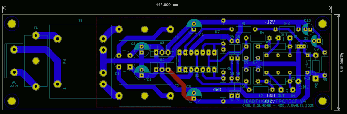
This is what the protection board might look like. By the way, does the time delay cap really need to be a bipolar? I somehow cannot figure out why it should be... Any thoughts, anyone? Cheers, Alex.

-
Great! I think I got the missing diodes... odd, though probably irrelevant: the middle resistor in the reference voltage divider is 500 ohms in your schematic and 1k in the gerber silkscreen.
-
Thanks Kevin! From the information that I could pull from existing information in the original thread and the google-drive I have tried to compile attached schematic. There were no gerbers or other layout files or images available. The file "protector3.PDF" seems to be missing all the diodes... can you please advise? I had to delete the previous schematic images due to upload file size limitations... sorry for that! Cheers, Alex.
-
Interresting... This one, right? Unfortumately, I was not able to find any schematic. Do you have a working link? Thanks!
-
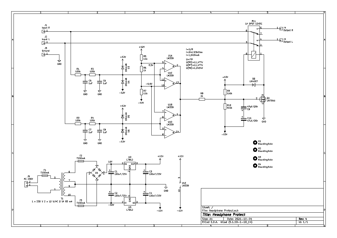
I continued to work on the protection circuit and came across the XEN SHPP Headphone Protection Circuit project: http://xen-audio.com/documents/SHPP/XEN%20SHPP%20V1.pdf Here, a potential flaw in the Epsilon 12 circuit is discussed that might result in the original design not to detect DC offset in certain situations. The outcome is that each channel gets its own DC detector and combines the outputs via diodes to the delay and relay circuitry. Also, in my opinion, the time delay cap C7 does not need to be an non-polarized electrolytic... am I missing something? The last mod is to drive the relay solely from the +12V DC to GND. As I have done away with the virtual ground concept, the rail-to-rail concept of AMBs design is no longer needed. If someone could please have a look at the schematic an comment if I have some bonehead mistake? Sorry about the bad resolution of the schematic - the forum only allows me to post images with a maximum size of 22.87 kB. Does anyone know, why that is? Thanks a lot - cheers, Alex.
-
A bit of progress this evening: here is the first schematic of the headphone protection circuit. As mentioned, based on the design of AMBs ε12 muting / protect circuit, https://www.amb.org/audio/epsilon12/ I removed his power supply and added an own simple +/- 12V version based on 7812 and 7912. It is deliberately weak on caps so that the supply will break down virtually immediately after power is removed via the mains input switch. Ah.. this circuit has its own tiny mains transformer!
-
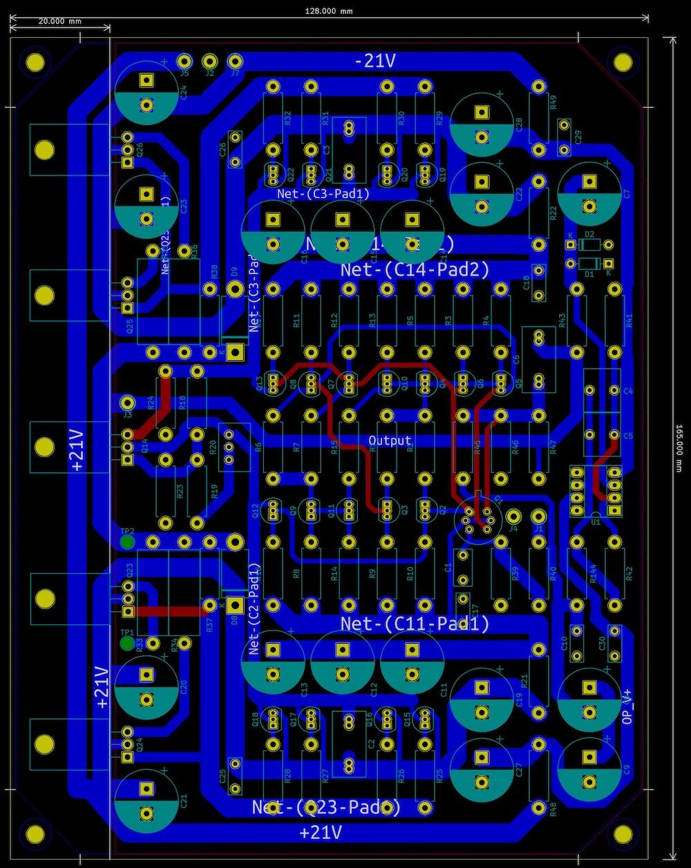
Indeed, the routing of the HT-rails is somewhat complicated, but my initial goal was to stick to the exact sequence of components as indicated by the original layout. I agree, that tidying up here and re-arranging to be more streamlined might be the way to go. The effects on the performance will probably be negligible. Regarding the arrangement of power output devices, the effect of mixing them up might not be worth the effort. If it saves some space I might consider this. Output protection circuitry is definitely a must! However a pure power on delay is too little. I was thinking of incorporating a protection circuit as outlined by AMB in his Epsilon12 muting delay & DC offset protection circuit. However, I will offer up a separate power supply for this with rather weak filter caps to ensure that the relays will drop off immediately after power off. Pulling current from the amps heavily buffered HT-rails is not a good idea in my opinion and fixing this issue by introducing a breaker contact parallel to the AC input power switch is not practical. Here in Germany we are required to break 230V power with both power leads (phase + neutral) and normal switches rated for mains voltage never come with more than two poles. Another option that I might include in the additional pcb for DC-protection is the addition of a DC blocking capacitor in the audio input path. Yes, I know there are many opinions on this topic out there. But after reading up on the topic in my favorite books "Small Signal Audio Design" and "Audio Power Amplifier Design" by Douglas Self, one sentence by Doug stayed in my memory: "In some respects, any DC-coupled power amplifier is an accident waiting to happen." He has also done respectable research on the effects of all kinds of electronic components and comes to the conclusion that coupling or DC blocking capacitors have no effect on linearity as long as they are installed in the low voltage or input side of an amplifier. Anyway, I want to give DC blocking a try and if I personally cannot hear a difference to the DC coupled version, then I will rather be on the safe side ... I like my headphones very much! And as a final note, I will definitely give the mods by my name twin above a go and see if I can even hear a difference!! Cheerio, Alex.
-
From now on my build will continue over in the "KSA-5 inspired amplifier builds"...
-
Reply Post from alexcp: The complexity of power traces looks excessive to me and suggests that an improvement could be made. If this was my board, I would try to shake it a bit, simplify, streamline, and make it more elegant. As an idea, you can try a different order of output transistors - instead of NPN-NPN-Thermal-PNP-PNP, something like NPN-PNP-NPN-PNP-Thermal, with power rails, the output trace and the ground running parallel to the edge of the board. This will bring in a different layout, which may (or may not) be helpful. Unless you plan to use some kind of off-board headphone protection, it would make sense to put the relay back. If you're not religious about the schematic, I'd suggest making the relay work for headphone protection, not just for turn-on delay. The amp seems to be reliable, but if you can avoid ruining some expensive headphones, why skip it? And of course - what would you expect - it would be great to make it possible to implement my mods (described above) on the PCB. It only takes two extra resistors and two small capacitors per channel, but the results are totally worthwhile.
-
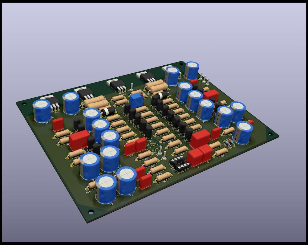
Hello everyone, I had started to post my attempts to build a modified KSA-5 klone over in the "krell ksa5 klone" thread, when I realized that I should create an own topic because my build would not be an exact clone... so this here is then exactly that. I will copy the previous posts here and delete there! Cheers, Alex. Hey folks, here is a first view on my take of this amplifier. I want to be able to attach the power transistors on one side via an L-bracket to a single heat sink. The power distribution sequence layout was kept in place but of course I had to do a little re-arranging. The original input stage is more or less unchanged. Both the top and the bottom layers have copper fills for the ground plane. I omitted the relay circuits as I plan to do a separate pcb for this. The project was done in kicad. I redrew the schematic and created a fresh pcb. Just to be clear: I do not intend to make money off this and will post all source files free whenever the project has turned out to be a success. Kudos to everyone for the excellent work and efforts previously put into this project! I hope I can somehow contribute with my ideas. I would be very interested in your comments - many thanks in advance! Cheers, Alex.
-
A question to one of the forum administrators: is it a good idea to move my posts starting on the 25th of September to a separate thread? Maybe called "KSA-5 inspired amplifier builds". I think I saw a few posts where some forum members wanted to keep this thread a more 'pure' clone build. Thanks.
-
Indeed, the routing of the HT-rails is somewhat complicated, but my initial goal was to stick to the exact sequence of components as indicated by the original layout. I agree, that tidying up here and re-arranging to be more streamlined might be the way to go. The effects on the performance will probably be negligible. Regarding the arrangement of power output devices, the effect of mixing them up might not be worth the effort. If it saves some space I might consider this. Output protection circuitry is definitely a must! However a pure power on delay is too little. I was thinking of incorporating a protection circuit as outlined by AMB in his Epsilon12 muting delay & DC offset protection circuit. However, I will offer up a separate power supply for this with rather weak filter caps to ensure that the relays will drop off immediately after power off. Pulling current from the amps heavily buffered HT-rails is not a good idea in my opinion and fixing this issue by introducing a breaker contact parallel to the AC input power switch is not practical. Here in Germany we are required to break 230V power with both power leads (phase + neutral) and normal switches rated for mains voltage never come with more than two poles. Another option that I might include in the additional pcb for DC-protection is the addition of a DC blocking capacitor in the audio input path. Yes, I know there are many opinions on this topic out there. But after reading up on the topic in my favorite books "Small Signal Audio Design" and "Audio Power Amplifier Design" by Douglas Self, one sentence by Doug stayed in my memory: "In some respects, any DC-coupled power amplifier is an accident waiting to happen." He has also done respectable research on the effects of all kinds of electronic components and comes to the conclusion that coupling or DC blocking capacitors have no effect on linearity as long as they are installed in the low voltage or input side of an amplifier. Anyway, I want to give DC blocking a try and if I personally cannot hear a difference to the DC coupled version, then I will rather be on the safe side ... I like my headphones very much! And as a final note, I will definitely give the mods by my name twin above a go and see if I can even hear a difference!! Cheerio, Alex.
-
Hey folks, here is a first view on my take of this amplifier. I want to be able to attach the power transistors on one side via an L-bracket to a single heat sink. The power distribution sequence layout was kept in place but of course I had to do a little re-arranging. The original input stage is more or less unchanged. Both the top and the bottom layers have copper fills for the ground plane. I omitted the relay circuits as I plan to do a separate pcb for this. The project was done in kicad. I redrew the schematic and created a fresh pcb. Just to be clear: I do not intend to make money off this and will post all source files free whenever the project has turned out to be a success. Kudos to everyone for the excellent work and efforts previously put into this project! I hope I can somehow contribute with my ideas. I would be very interested in your comments - many thanks in advance! Cheers, Alex.
-
Greetings gentlemen, in search of a fun project I found this thread and really want to give this project a shot! Unfortunately all of Kevins links to the source data for the amp are dead... can someone help me out here? Thanks a lot - cheers, Alex.