
Bespav
-
Posts
32 -
Joined
-
Last visited
Recent Profile Visitors
2,237 profile views


Bespav's Achievements
Advanced Member (3/6)
1
Reputation
-
Hi, JoaMat! Very nice PCB routing concept. Something similar: Let's go ahead, it's time to provide DIYers with the next features: 1. A simple swapping JFET/BJT input stage on the mezzonine with standartized fitting place/connector. 2. Really smaller dimensions with easier through-pcb-screwing. 3. Integrated onboard fitting connector for corresponding voltage regulator. 4. Check transistors availability and, of course, create different versions of the output stage, one for TO-126, other for TO-220 devices and maybe one for TO-3P/TO-247/TO-264. 5. Since you have provided bias control it's time to make output stage 2-stage emitter follower, vertical mosfet source follower or lateral mosfet source follower for those who want to experiment. 6. Input JFET transistors have cascodes, so aren't we ready to provide cascodes for VAS devices? 7. VAS devices on the main heatsink and also an option of the TO-126/220 cases. 8. Really higher dedicated IPS/VAS supply rails, up to +-150 volts. 9. An option to use modern low-ESR solid polymer capacitors for the power stage. 10. Dedicated input stage before volume regulator for common mode error rejection. 11. Second order integration filter for output nulling. So, the concept. Mezzonine construction. One PCB for JFET/BJT input stage and corresponding cascode devices, second PCB for one OPS shoulder and third PCB for the voltage regulator. All for as-LEGO-construction as possible.
-
Ok. This one? https://www.ebay.com/itm/8-X-NEC-2SK163-2SK163L-2SJ44-2SJ44L-AUDIO-FET-/383673522014?_trksid=p2349624.m46890.l49292 Politicizing and nationalizing are sad. Mostly the same if i try to buy lateral FETs from British's Profusion. All those jfets and mosfets are the last of Mohicans and it's even more sad.
-
No, there are two different individually biased input stages and no need to match n- with p- devices.
-
Since you're on the audio slippery track there are no ways to turn off. Yes, you can use bc850c/bc860c or even cheap as dirt 2n3904/2n3906 on the input stage and obtain similar **measurable** performance. But JFET input stage sounds better. It's like to changing Samwha capacitors to a purebred Elna Silmic. Really we don't understand what to measure to obtain sonic-correlated ruler/scale.
-
Try here: https://www.ebay.com/itm/Toshiba-2SJ74-2SK170-Quad-0-03-4-9-11-bl-B-/253517005056?_trksid=p2349624.m46890.l49292
-
Aaaaargh, folks... Don't you want to heat your soldering irons? Start your milling machines? Turn on oscilloscopes?
-
Hi, Folks! Aren't there a time to try something new? What a headamp would you like to try? Of course, A-Class, of course "No Miller capacitance", of course "Balanced". Do we need new beasts? Aren't there a time to brainstorm or public dispute for the new designs?
-
Nichikon NU and L8 series are in most interest due to voltage rating up to 63 V with more than good ESR and more than enough capacitance. Yes.
-
Put solid-polymer caps with appropriate diameter at a 100 uF places and PP/PE caps can be left unpopulated.
-
1700V N-type SiC MOSFETs are freely available for something like ten dollars, do you really need more?
-
Let's be honest with each other. Not to this kind of ugly build. The bicycles are already invented and now we can only polish their lacquer or grease their chains. Level achieved already a way higher of common soldering skills or schematic understanding. Let's confess, no need to run further and we stomp at the spot.
-
State of the art of the heartless bitches... But, cmon, your designs are so bulletproof, that can resist such a build! Now there are only one approach in public linear design. Boards splitted to cheap 100x100mm and opened to order through jlpcb or similar. Kit of the reliable parts are available through ebay. This will result in a small quantity of badly copied fakes but keeps badly assembled/builded. Also SMD machine-assembled design could be a way to minimize those fake capacitors and trannies with 100 pF collector-base capacitance. Times when one can pick well-known design and sell 1k builds are finally gone.
-
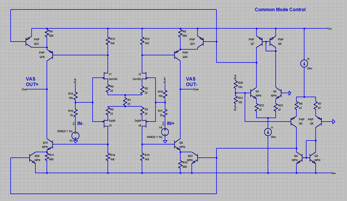
Keeping in mind Kevin Gilmore's design rules i have insomnia about stabilizing common mode of JFET input stage without sacrificing CMRR or straight referencing it to the amplifier/source ground. So, check attached schematic. While keeping straightforward signal flow aka "Gilmore's gesign rule" it also have second control loop which helps SuSy amps to maintain output common mode near ground potential.

-
Hi, Kevin! Your site is down or moved somewhere?
-
Could someone help me find out if these 2SK369V are real?
Bespav replied to sbelyo's topic in Do It Yourself
Yes, i have buyed 2SK163/2SJ44 pairs from this seller, they was original and very well matched. Matching checked with PEAK Atlas DCA75 And gate capacitances checked with simple transistor tester (as a marker of datasheet specs): Combination of the transconductance and gate capacitance are unable to be counterfeited together. It would be great to check intrinsic device noise, but i'm too lazy for that. So i hope, those 2SK369's are original too.