Shawn
Returning Member
-
Joined
-
Last visited
Everything posted by Shawn
-
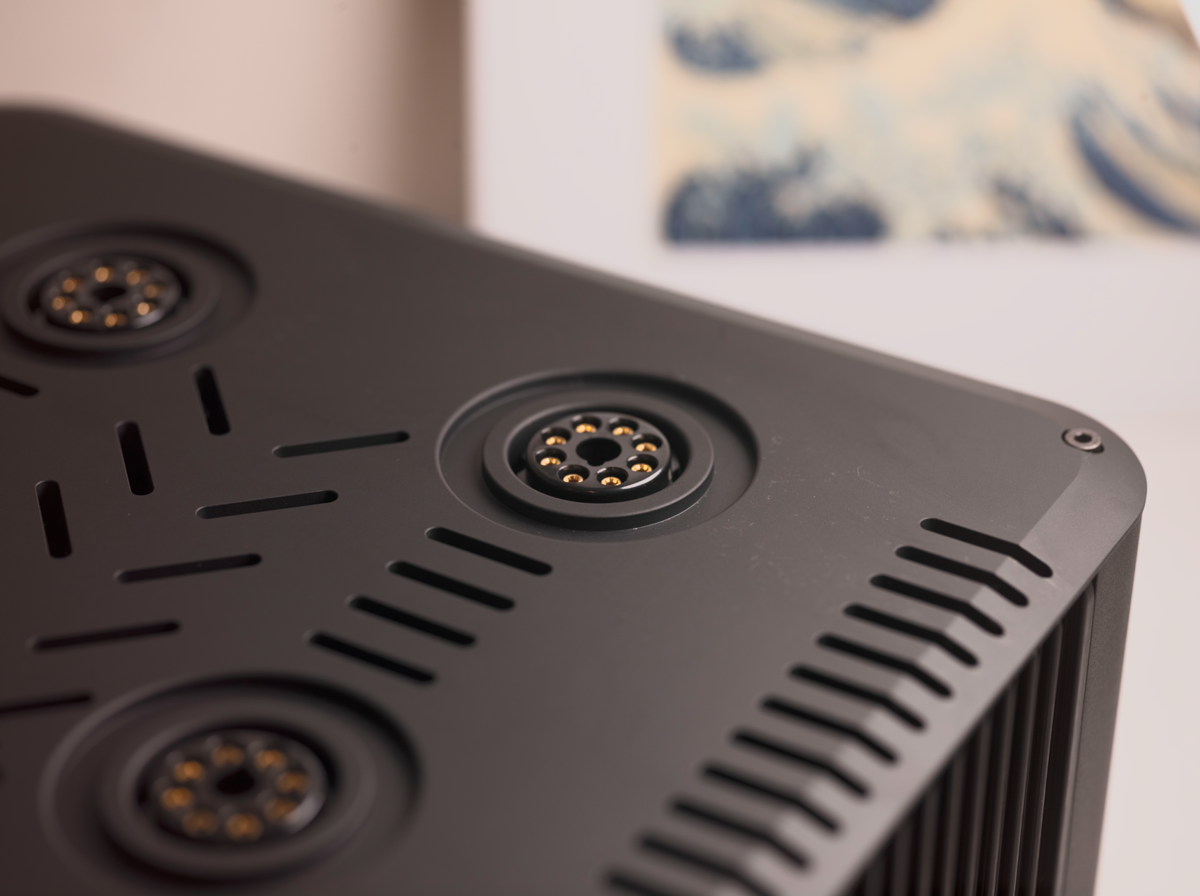
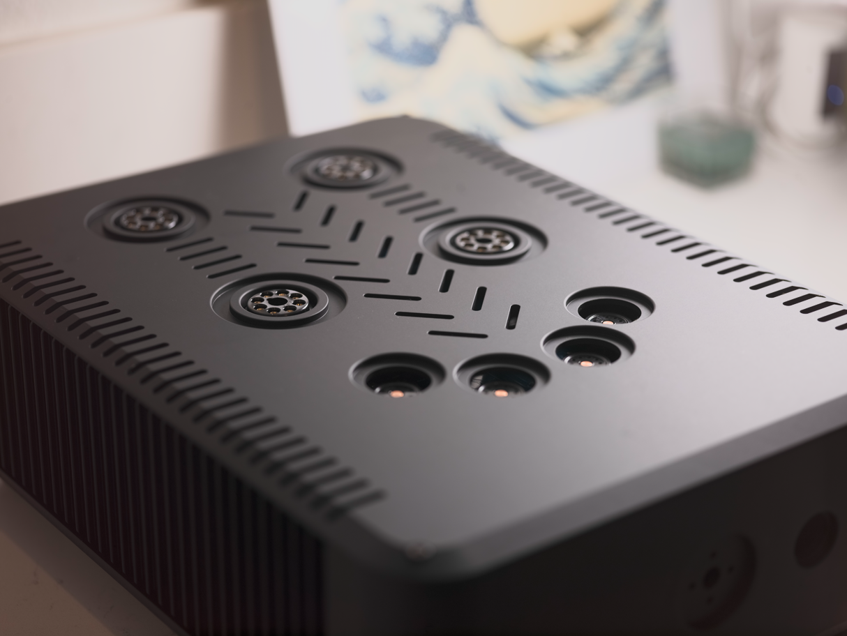
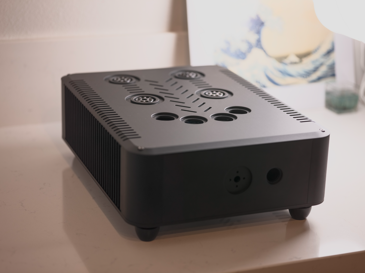
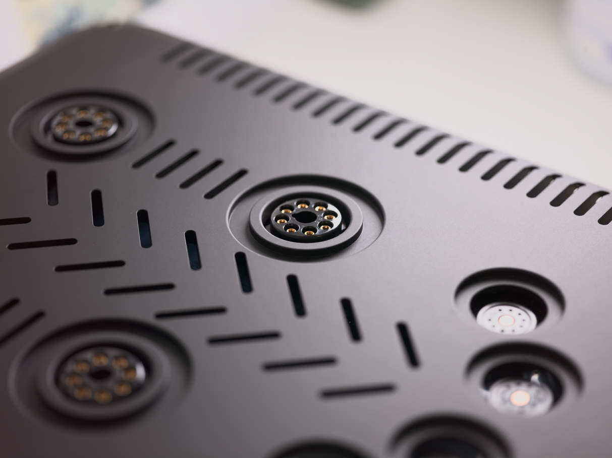
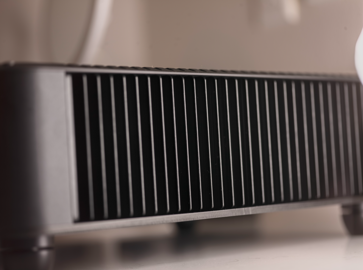
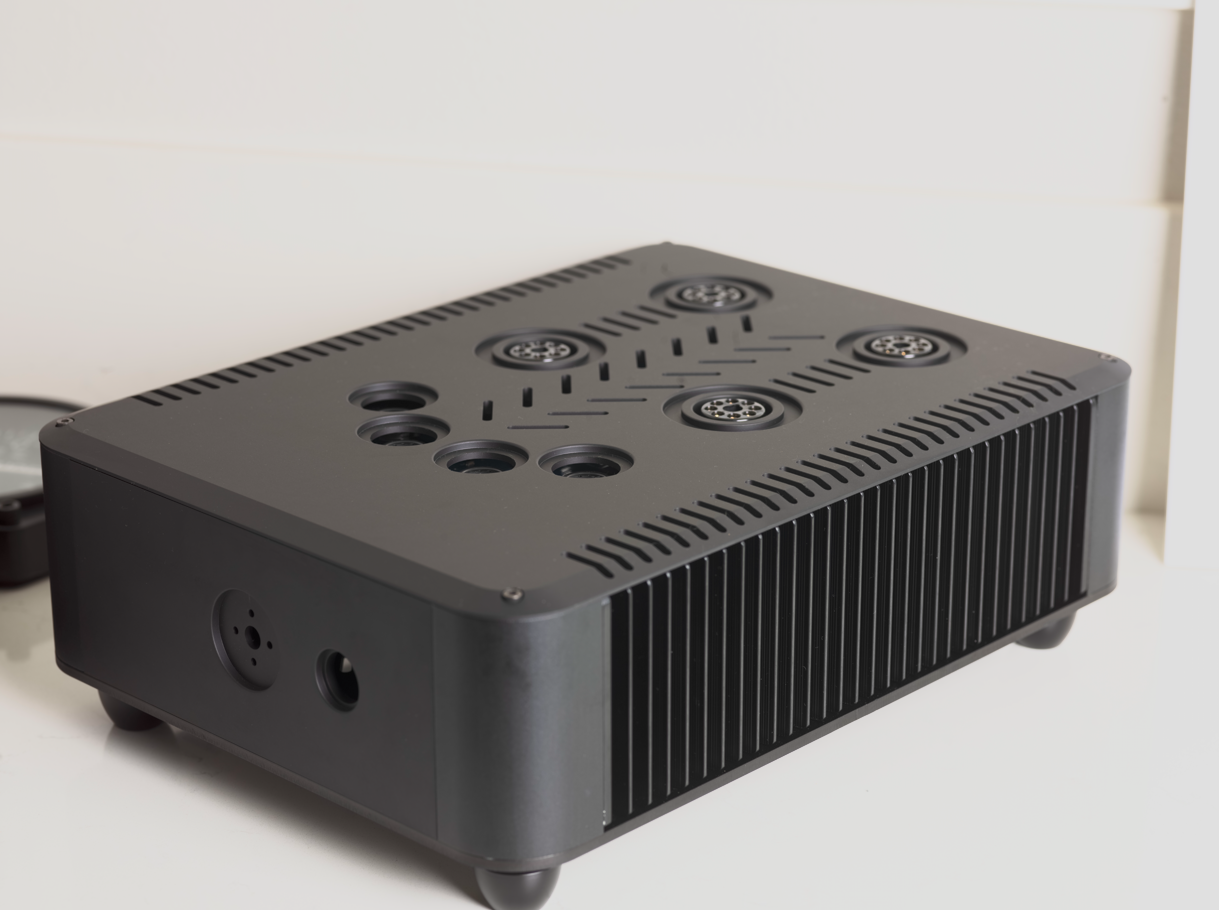
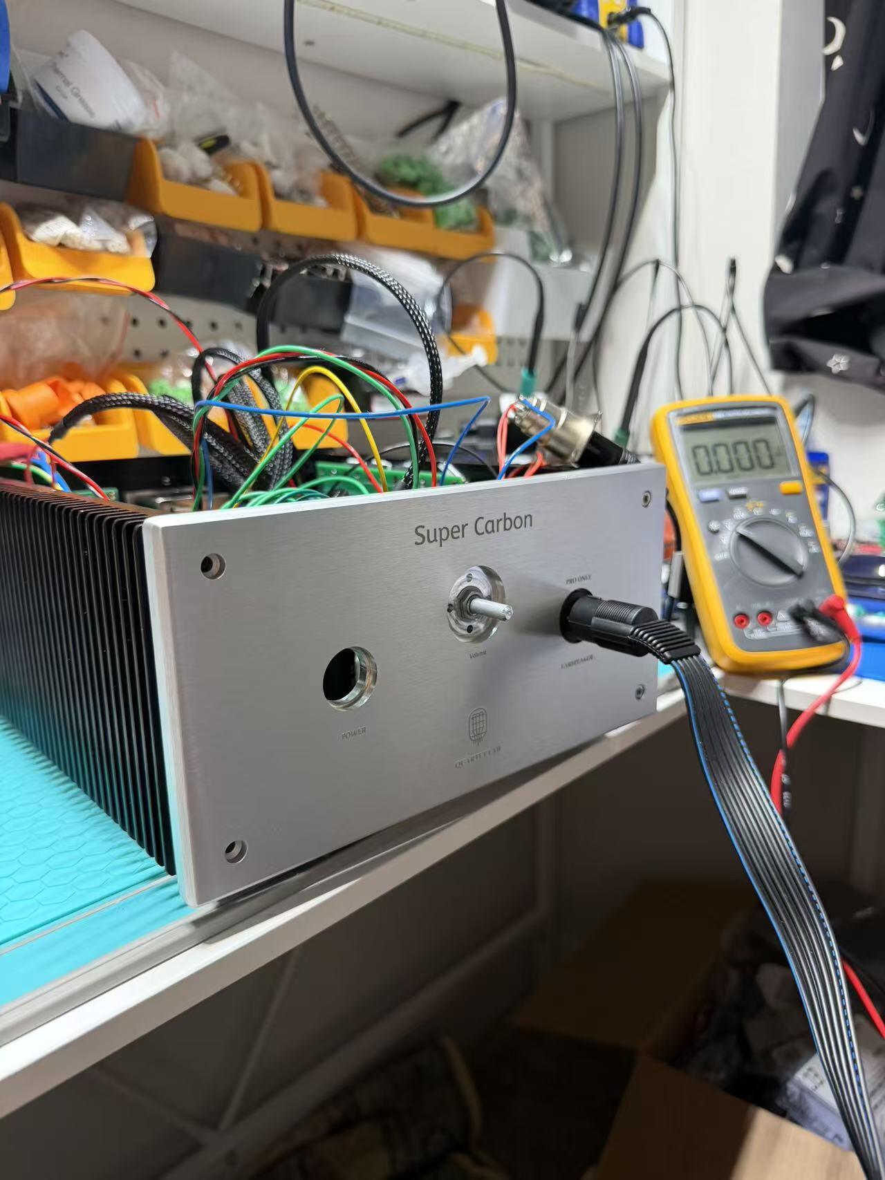
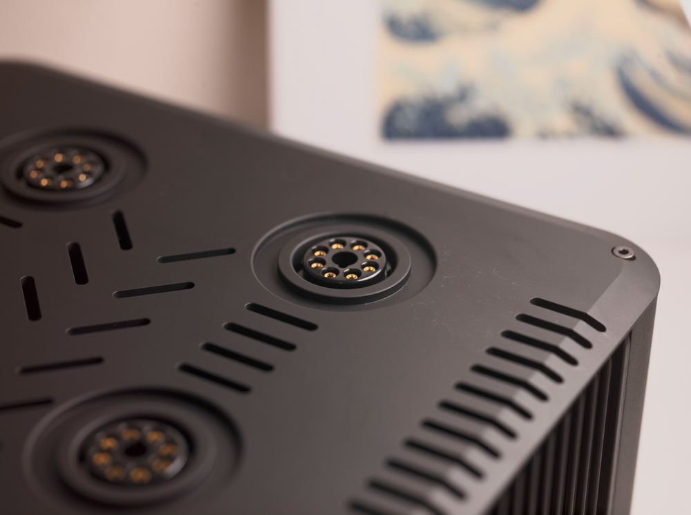
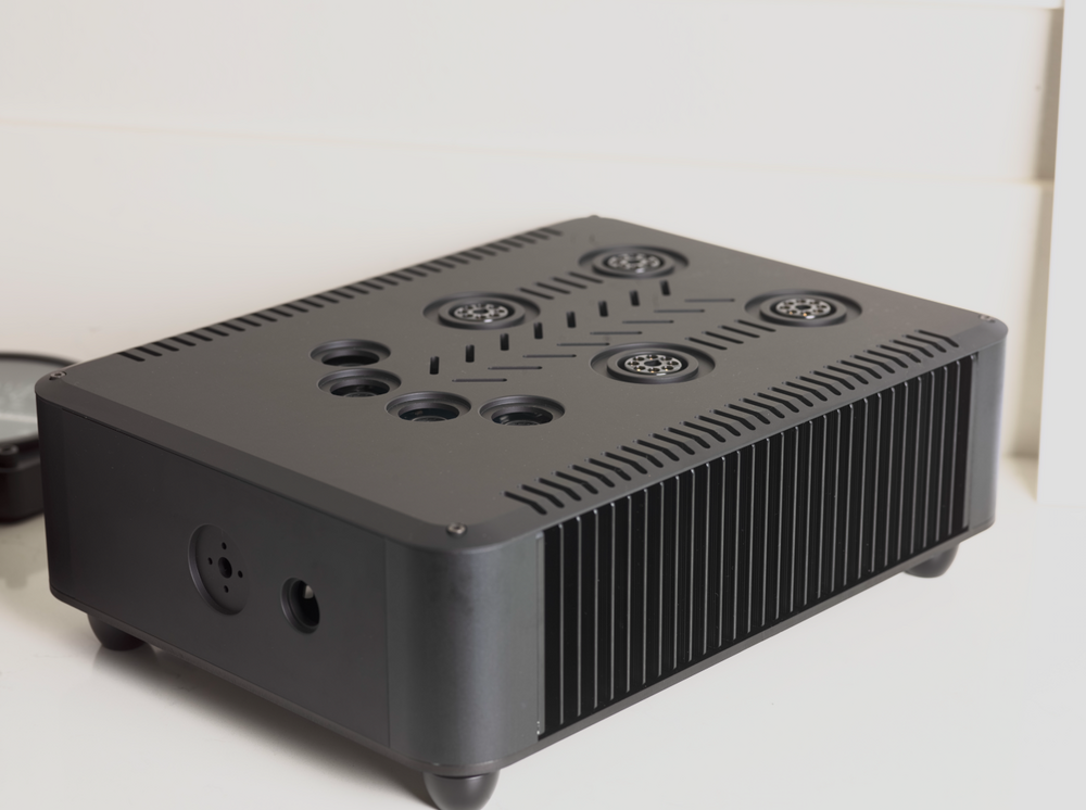
Both the power supply and amplifier chassis are approximately 290 mm × 400 mm × 90 mm, so it's actually fairly compact considering it's a full-size T2. The power supply uses five GRHV regulators and features plug-in bias daughter boards, making it easy to switch between different bias voltages. Right now it supports both Normal Bias and Pro Bias outputs. The PSU also includes about a 50sec high volt soft start. In addition, there's an AC inrush limiter on the mains input. After roughly one second, a relay bypasses the current-limiting resistor, reducing the inrush current seen by both the filter capacitors and the tube heaters during startup. On the amplifier side, most of the passive components are SMD, which helped reduce the overall PCB and chassis size. The amplifier topology stays very close to Kevin's original T2 schematic, but I added support for several different implementation options to make the design more flexible. It supports three different CCS configurations:10M90, 10M90S + DN2540, and the original T2 complex CCS. The active battery section is also configurable. It supports: LED string reference, LT1021 reference. For the 2SK216 and 2SJ79 positions, I added an extra pin so they can be replaced directly with TTC and TTA devices without modifying the PCB. The overall goal wasn't to redesign the T2, but rather to preserve the original circuit while making it easier to build, maintain, and adapt as some of the original parts become increasingly difficult to source. The chassis is CNC machined by a local machine shop. One detail I paid particular attention to was the top cover of the amplifier chassis. I designed it so that the EL34 tube sockets sit perfectly flush with the top panel, which I think gives the amplifier a much cleaner appearance. Additional ventilation slots were added in the center section for airflow. The side heatsinks are sandwiched between the top and bottom panels. This not only gives the chassis a cleaner look and prevents the sharp heatsink fins from being exposed, but also makes it much less likely that you'll scratch your hands when moving the amplifier. To make sure the heatsinks can still dissipate heat efficiently, I also added ventilation openings in the top and bottom panels wherever they cover the heatsinks. I've also been thinking about turning this project into a group buy, although I'm not sure how much interest in the T2 still exists today. The main motivation would be to reduce the chassis cost, since having a single custom CNC chassis made is quite expensive. If enough people were interested, the machining cost could come down significantly.
-
After about a year of work, I've finally finished redesigning the PCB layout for the original T2. The new layout supports several different active battery implementations, as well as multiple CCS options, making it much more flexible for different builds and future experimentation. I've also completely redesigned the chassis. Like the original concept, it will still use a two-chassis configuration, with the power supply and amplifier housed separately. It's been a long project, but it's exciting to finally see it coming together. I'll share more photos and progress updates as the build moves forward.
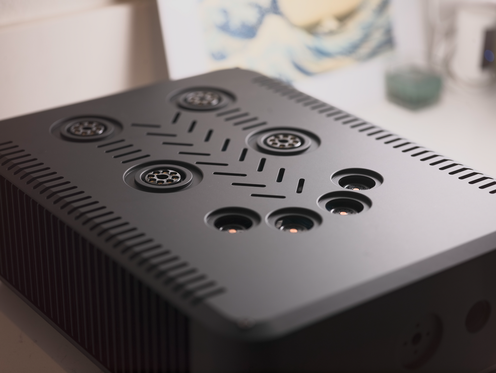
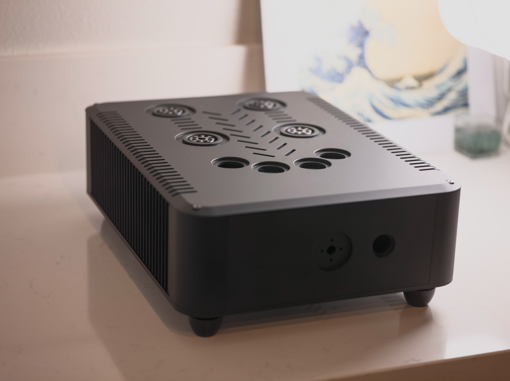
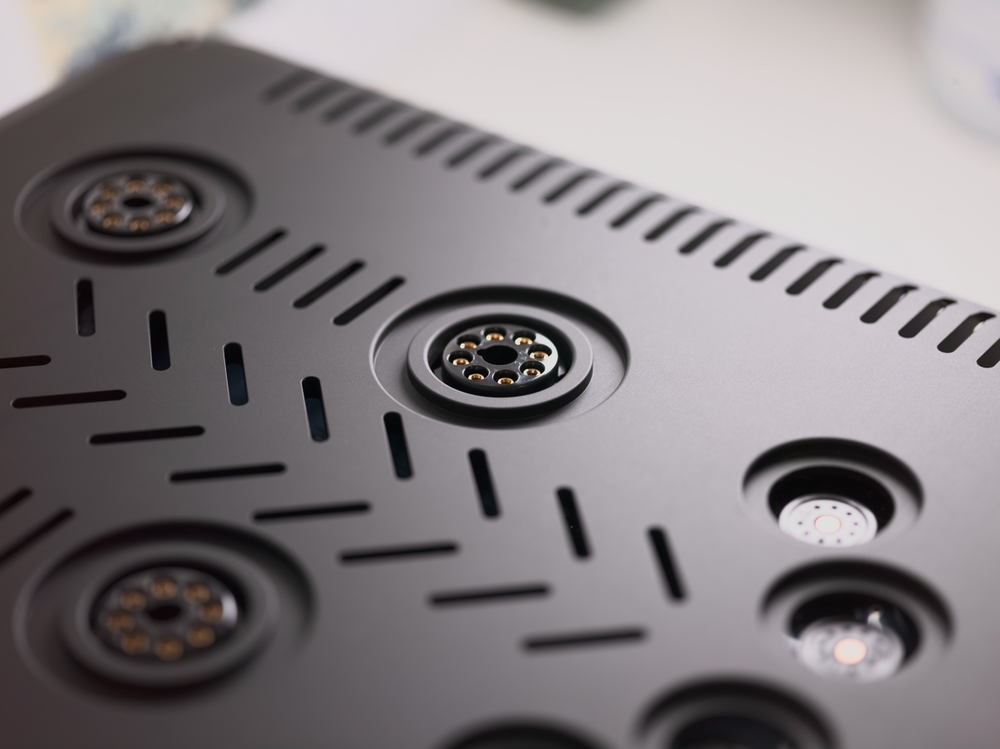
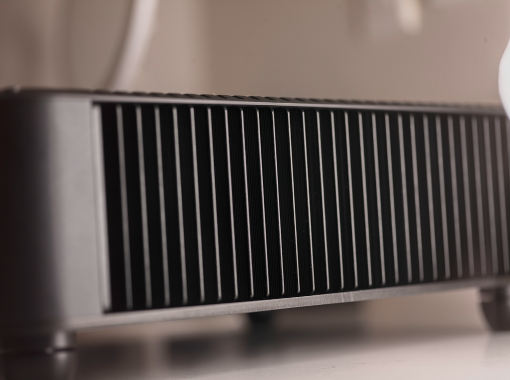
-
Okay, I finally confirmed the source of the problem today. It looks like the LSK389 input stage is simply extremely sensitive and is very easily picking up magnetic field noise from the power transformer.
-
Thanks for the information. It looks like 5pF is also stable on my build, although I’m using the SMD version of the power supply boards. When you mentioned the “dual current sources”, what exactly did you mean? Are you referring to the two current source stages before and after the power supply on Kevin’s latest board? I’m using PZTA42 for Q9/Q10 instead of TTC004A, so perhaps that’s something I should investigate next. I also have a pot at the input, just like your build. If you have access to an oscilloscope, could you check the O+ and O− outputs? On my board there’s a roughly 120kHz sine wave (it changed to around 96kHz after I experimented with MLCCs on the RKZE outputs), and it seems to be related to the isolated DC/DC supply. I’d be interested to know whether your board shows the same behavior, even if it’s not audible.
-
I checked the datasheet as well. Since I’m already feeding the converter from a GRLV, I don’t think the input side is the issue. One interesting thing I noticed is that the datasheet for a compatible replacement part (with essentially identical specifications) recommends adding an LC output filter for noise-sensitive applications. The example value is around 0.47µF on the output. I don’t have any 0.47µF MLCCs on hand at the moment, but I’ll probably place an order next week and give that a try to see if it helps reduce the remaining noise.
-
I ended up switching back to the 5pF capacitor. With 470pF, the nearby STN9360 starts behaving incorrectly, so something in my implementation clearly doesn't like that value. I replaced the output capacitors on the switching supply with four 0.1µF/50V MLCCs, just as Kevin suggested. After doing that, the ripple on O+ and O− at around 120kHz dropped to roughly 96kHz. At this point it seems like the tiny residual hiss may actually be related to the switching supply rather than the amplifier itself. What I'm not sure about is whether a 120kHz switching component could somehow be demodulated or otherwise make its way into the audible band.
-
Just to confirm, do you mean adding a .1 to 1 uF ceramic capacitor directly across the RKZE-1515 isolated supply output (+15V to -15V) that powers the CCS section?
-
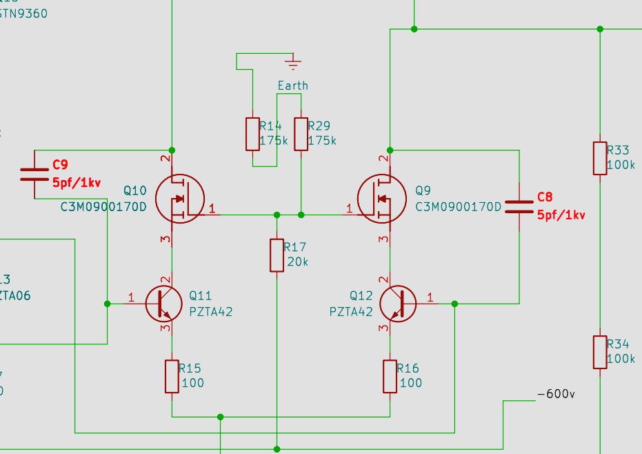
A small update on the Super Carbon debugging. Today I tried shorting IN+, IN−, and GND together at the input. The background noise was reduced, but there is still a very slight residual hiss that I can't completely eliminate. It's extremely low that you can only hear it if you put your ear right up against the headphone. Because of that, I'm starting to think the input stage may not actually be the source of the remaining noise. I'm wondering if it's possible that the compensation around the C3M0900170 devices is involved instead. Specifically, I'm referring to the 5pF capacitors C8 and C9 connected around Q10 and Q90. Could insufficient compensation there contribute to this kind of residual noise? @kevin gilmore , I'd really appreciate your thoughts before I continue experimenting.
-
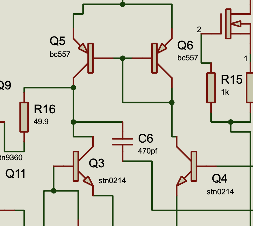
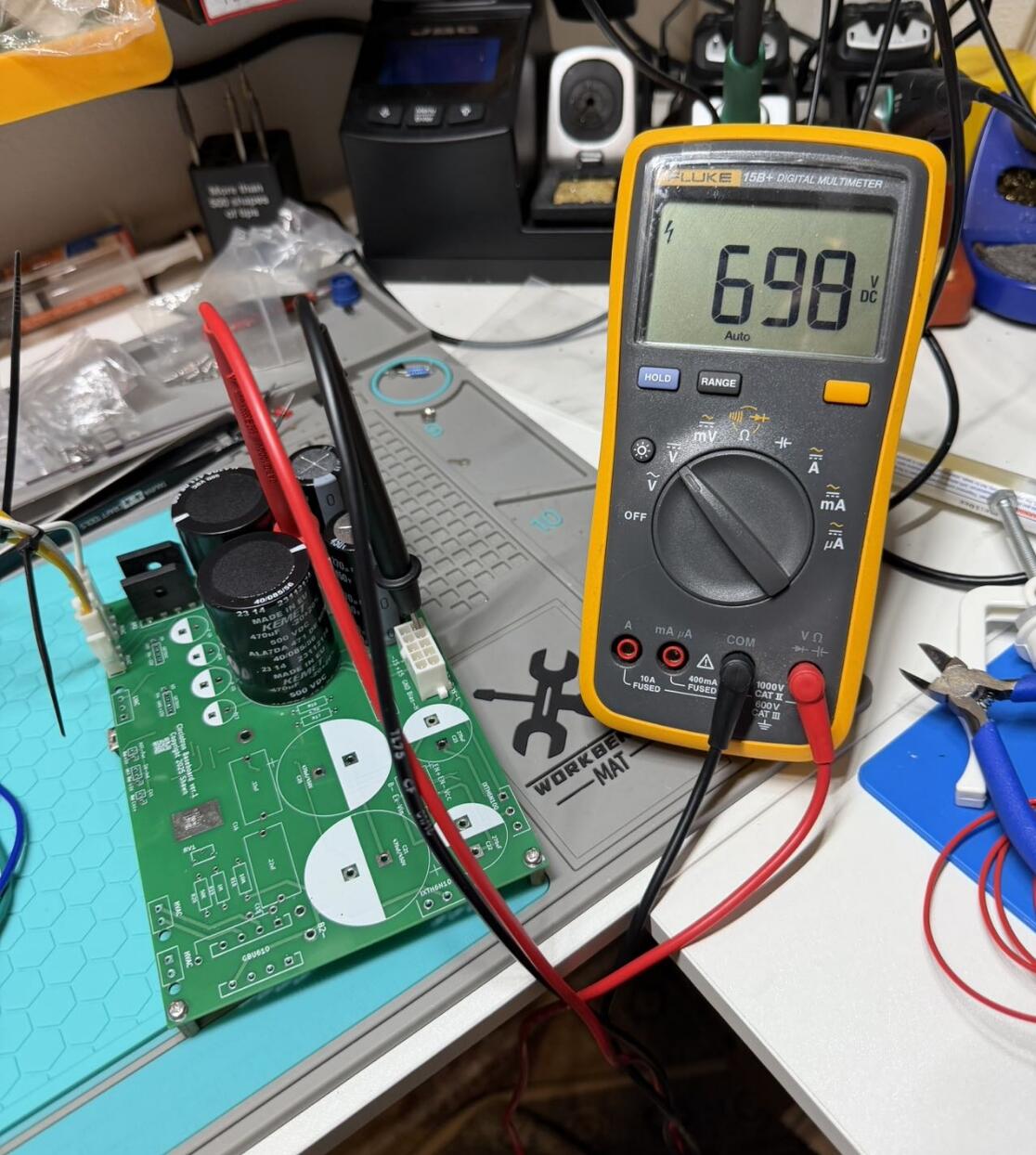
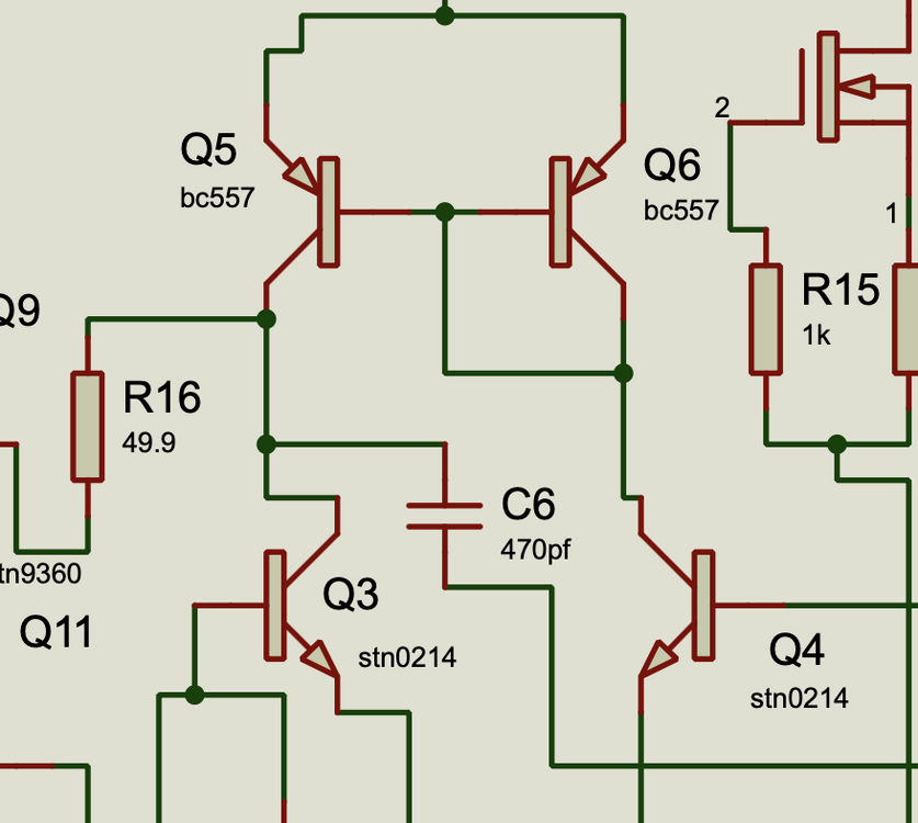
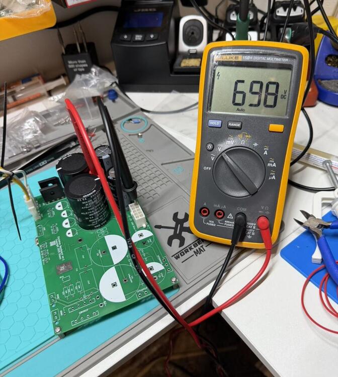
Yes, it’s the C6 470pF capacitor in the power supply. I originally installed a 5pF capacitor instead of the specified 470pF. After changing it to 470pF, the output voltage rises very close to the raw DC input. My raw DC is about 698V, while Vout increases to around 675V, instead of regulating to the expected 600V.
-
Thanks, Kevin. At the moment I only had 50kΩ resistors on hand. After replacing the input resistors with 50kΩ, the background noise is almost completely gone. There's still a very slight hiss/current noise, so I may also try adding a small pF-range capacitor to ground for some additional RF filtering. I also noticed something a bit strange with my layout. On my board, installing the 470pF capacitor causes the output voltage to rise very close to the raw DC rail, whereas using a 5pF capacitor doesn't cause that behavior. I'm not sure if it's layout-related or if I've made a mistake somewhere. Has anyone else run into this issue with their build?
-
A small update on the Super Carbon troubleshooting. After replacing the 5pF capacitor with the 470pF value shown on the schematic, the oscillation was reduced significantly. However, there is still a very noticeable background noise. At this point I'm starting to suspect the XLR input stage instead of the power supply. When I short IN+, IN−, and GND together at the input, the background noise disappears completely. That makes me think the input stage may simply be too sensitive. @kevin gilmore do you think it would make sense to reduce R48 and R49 from 500kΩ to something like 200kΩ or 100kΩ? Or perhaps add a small capacitor for some RF filtering at the input? I'd appreciate any suggestions before I start experimenting further.
-
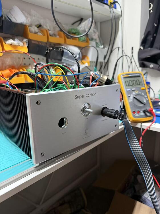
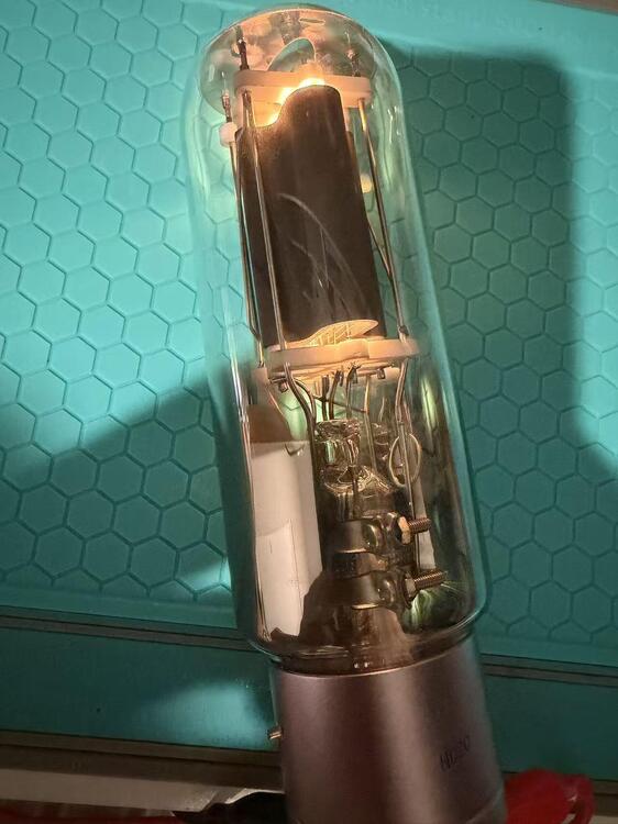
Last week I finished assembling the Super Carbon, and it's now up and running. The first listening impressions are very encouraging, but there is still some audible background noise that needs to be eliminated. At the moment I suspect it's related to the power supply compensation, possibly an oscillation. On the schematic, around the STN0214, there is a 470pF/1kV capacitor. I initially installed a 5pF/1kV capacitor there, so it's possible the compensation at that node is simply insufficient. I'm currently waiting for some mica capacitors to arrive so I can experiment with the compensation network. While simulating the circuit in LTspice, I measured approximately 540V VCE across the STN0214. Based on that, I don't think the PBHV2160(VCEO = 600V) is an ideal substitute for the STN0214, especially if you're targeting output voltages significantly above 600V. On another note, I also performed the initial testing of the D&G 211 filament supplies, and they appear to be working as expected.
-
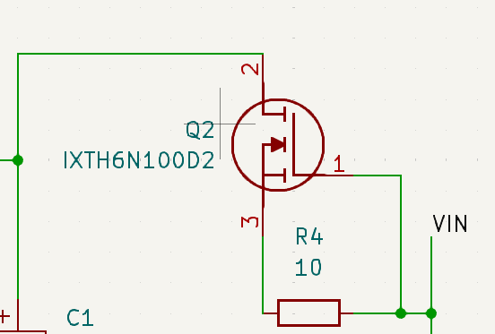
I believe you can change the value of R4 to adjust the current limitation. I_limit = Vgs / 10 A gate stopper may be added for better performance.
-
Hi, @MLA I'm planning to test this next month, and I have one more question: The low-voltage ±15V supply GND on the Carbon PCB is connected to the high-voltage GND. Does the ±15V supply also need to float somehow in this configuration, or should I simply connect the GRLV GND to the Carbon GND as normal? I'm trying to make sure I understand the grounding scheme correctly before I start wiring everything up.
-
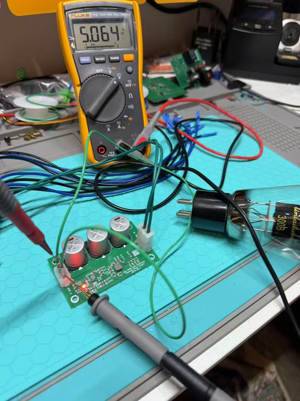
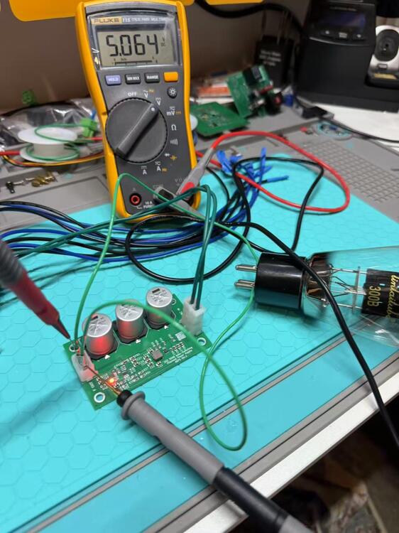
Did some testing today on the auto switch filament board. It seems to correctly detect 2A3 300B so far. For the test, I directly soldered the cable onto the 300B filament pins. I know that’s not the best practice, but it was quick.
-
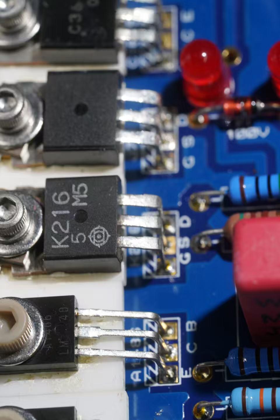
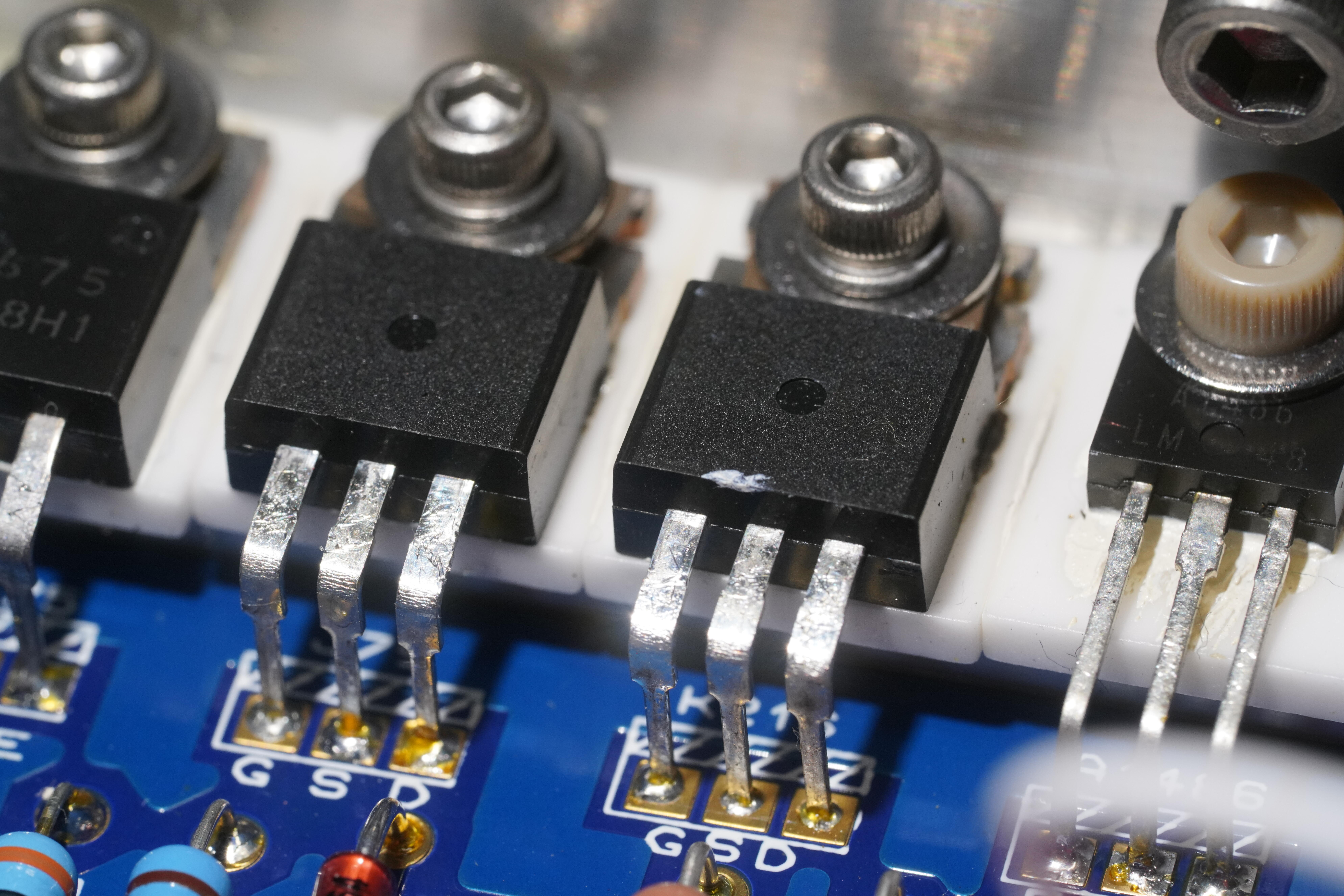
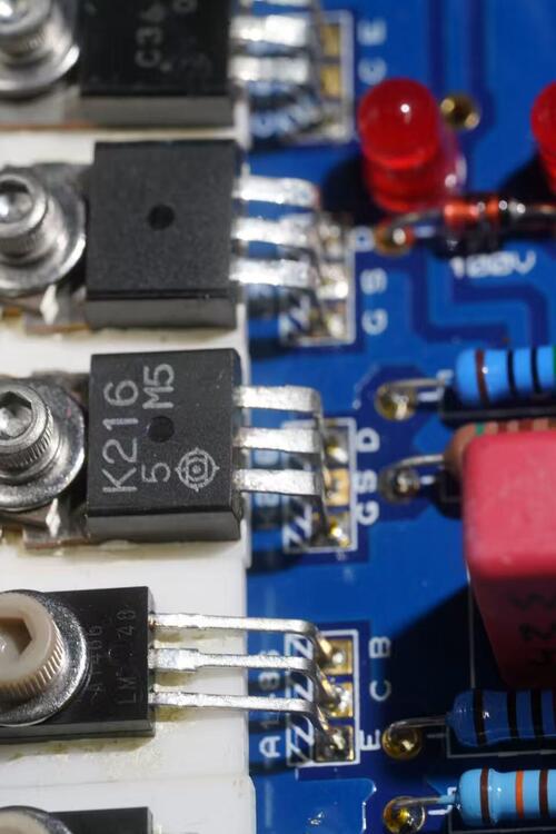
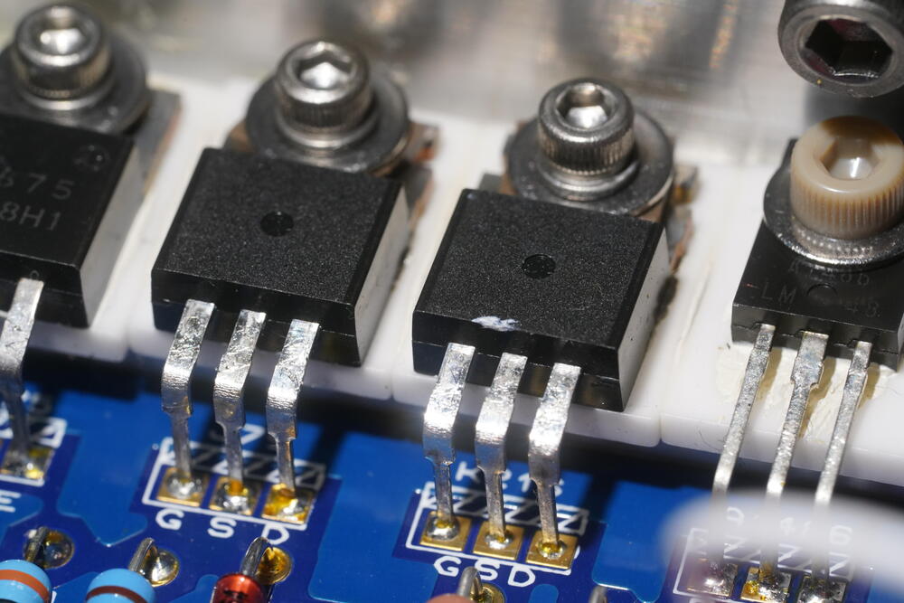
Thanks for your reply, Pars. The photo angle isn’t ideal. In real, at a certain angle under light, I can barely make out the 2SK216 / 2SJ79 markings, but they are extremely faint. I’ve seen genuine Hitachi versions before and they look quite different. I’m not sure if Renesas production ever looked like this, but I personally haven’t seen any sands with markings this faint. Below is a comparison. On one side is what I believe to be a normal 2SK216, and next to it is the suspicious 2SJ79. This T2 actually has a mix of both types of markings installed.
-
I’m currently helping repair a DIY T2, and while inspecting the amplifier section, I came across something a bit suspicious. The 2SJ79 / 2SK216 devices look like this (see attached photos). The marking on them appears very faint and somewhat unusual: not what I would normally expect from these parts. This makes me suspect that they might be counterfeit or at least not from a reliable source. Has anyone here seen this kind of marking before on genuine 2SJ79 / 2SK216? Any insight would be greatly appreciated.
-
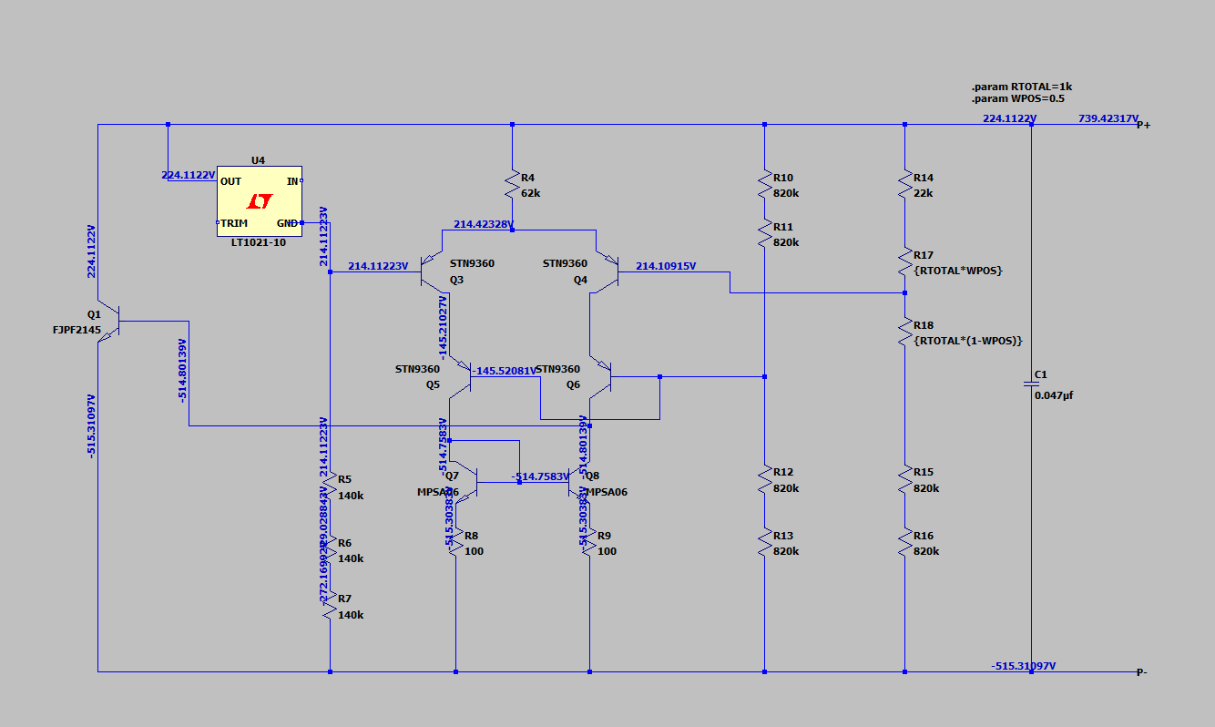
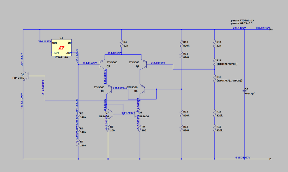
Thanks to @MLA for sending me a few FJPF2145s. To avoid turning them into smoke immediately, I’m currently still in the simulation phase. So far, the battery section appears to behave properly, at least in theory🙃 I’ll also try simulating a few alternative devices to see how they compare. From what I’m seeing so far, a Darlington configuration might actually make more sense in this position. More updates once I move from theory to reality.
-
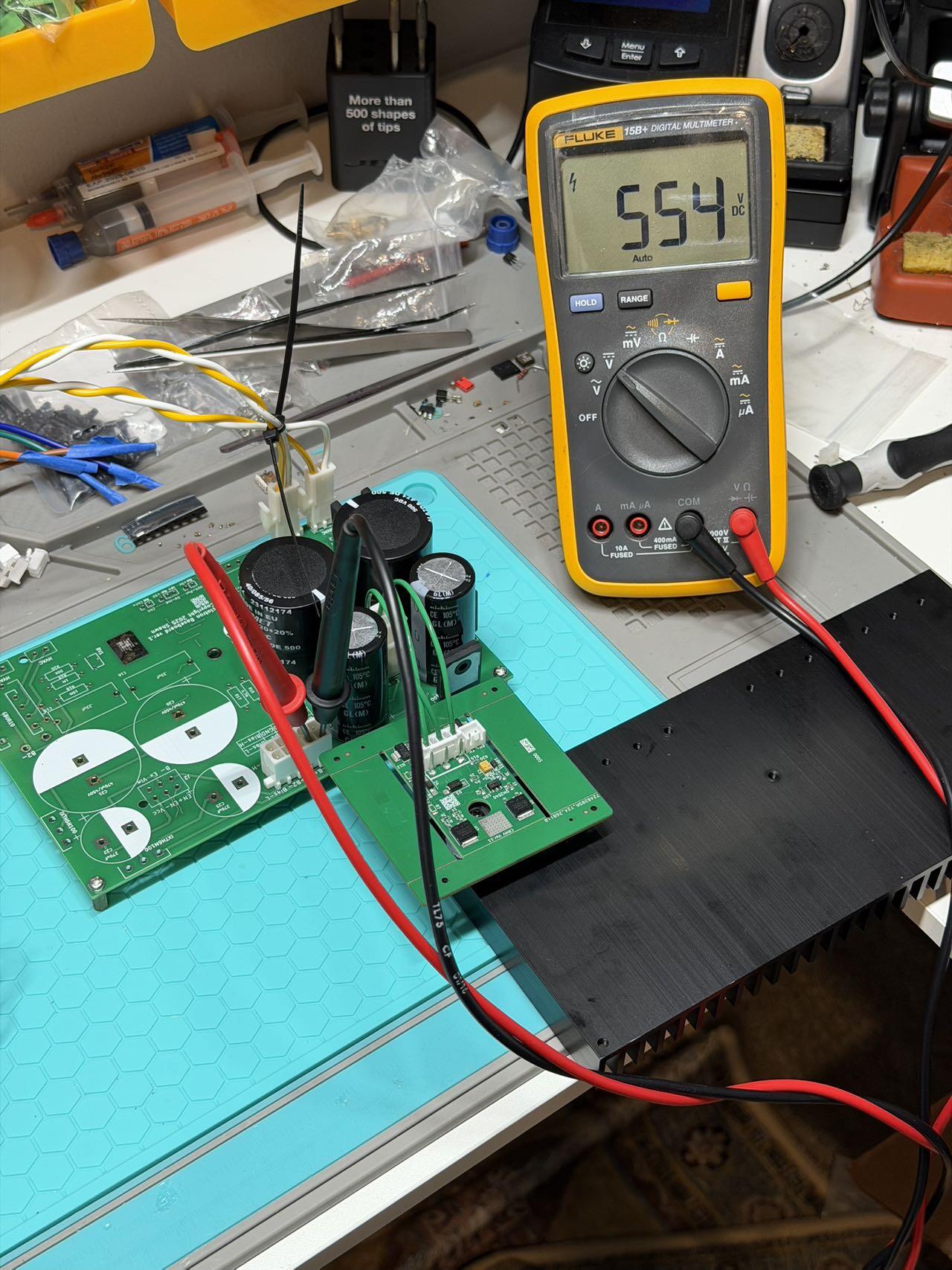
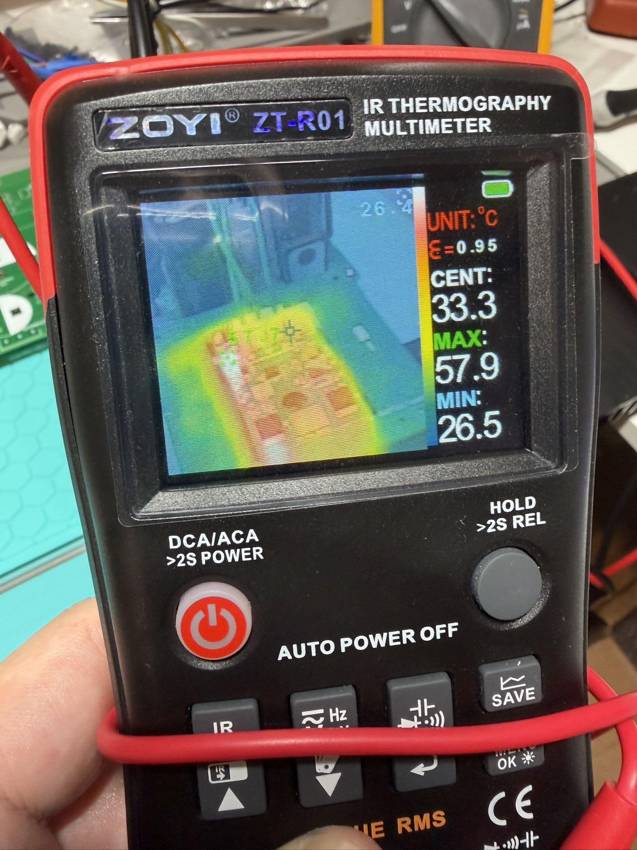
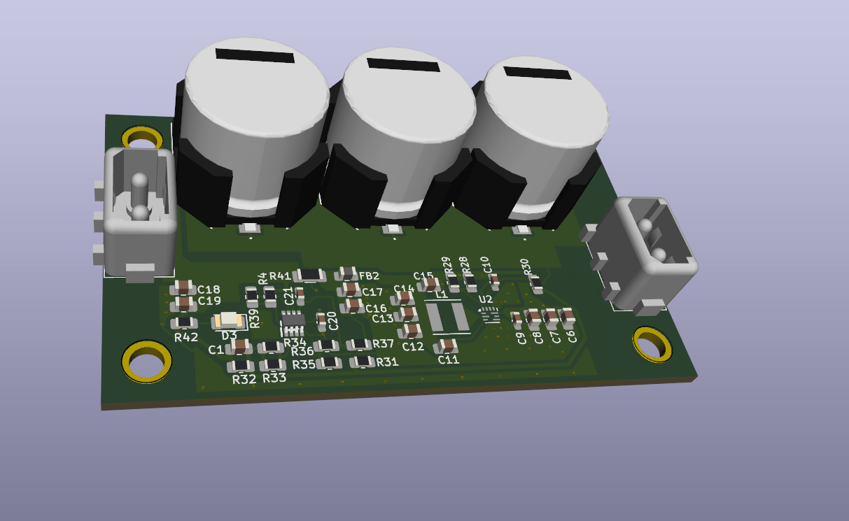
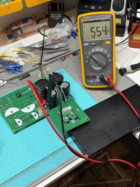
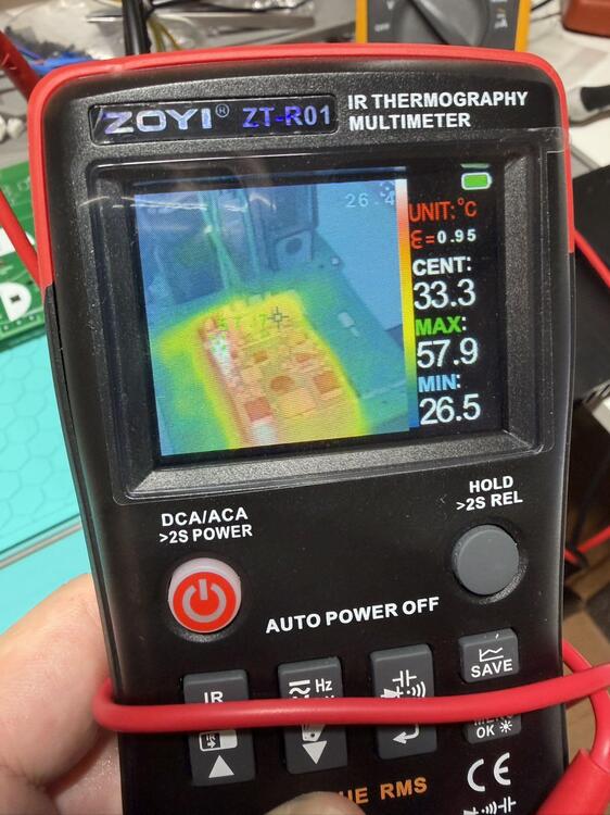
OK. Did a first power-up test for CRHV today. With 360k set for 550 V, I’m measuring about 554 V in practice. I only let it run for ~10 minutes. A quick IR check shows the CRHV peak temperature at ~58 °C. I suspect running it from dual 250 VAC inputs targeting ~600 V output may result in slightly better thermal behavior. At the moment, only the high-voltage section is populated. The delay soft-start and ±15 V sections are not installed yet, but they should function as expected once added.
-
It’s 2026 and FJPF2145 (and 2SC3675 in some builds) have been discontinued for quite a while. So far I’ve come up with a few candidates: KSC5026 BUL216 (I remember this being mentioned before) FJP5027 My main concern is output capacitance. I’ve seen comments that BUL216 has relatively high capacitance, and the other candidates seem in the same ballpark. Their Ic ratings are ~1.5A to 4A, and gain (hFE) looks acceptable. But I’m worried about any impact on stability. Has anyone actually tried one of those (or any other modern parts) as substitutes for FJPF2145 / 2SC3675? Datasheet attached: https://www.onsemi.com/pdf/datasheet/ksc5026m-d.pdf https://www.onsemi.com/pdf/datasheet/fjp5027-d.pdf https://www.st.com/content/ccc/resource/technical/document/datasheet/group1/01/eb/74/95/d4/55/44/6c/CD00000009/files/CD00000009.pdf/jcr:content/translations/en.CD00000009.pdf
-
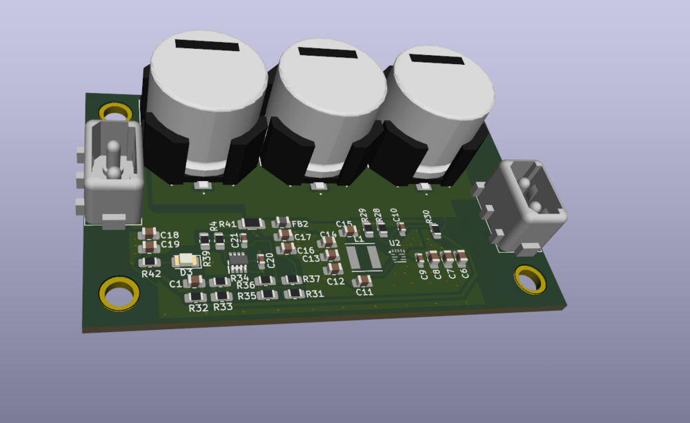
Did some work on the auto-switch filament board today. It’s based on the same schematic as before, but with additional rectification and filtering added this time. The mounting holes and overall dimensions are kept identical to my previous filament board, so it can be dropped in as a direct replacement without any mechanical changes.
-
Thanks a lot, JoaMat. Much appreciated.👍 That confirms my understanding.
-
@JoaMat I have a quick question regarding the servo. Once the servo is in place, does that mean the cathode resistor and its bypass capacitor are no longer needed, and the cathode is effectively tied directly without local bias components? Or are they still retained in some form? Thanks.
-
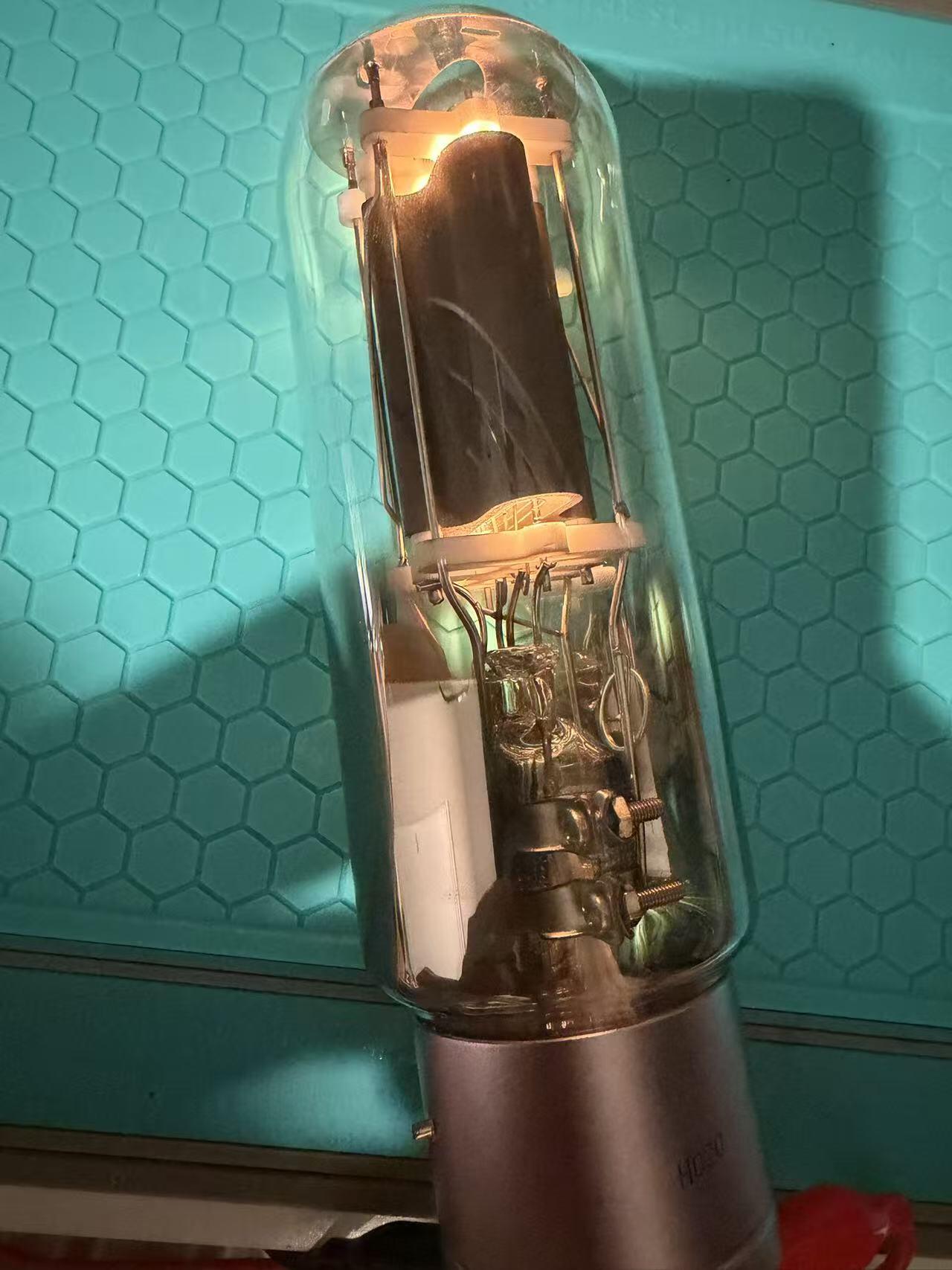
I haven’t really followed up on this for a while, but today I did a quick LTspice simulation of the 2A3 stage. With a constant plate current of about 23.8 mA, a 3100 Ω cathode resistor looks like a reasonable bias point (compared to 3300 Ω previously). The operating point itself is stable, and plate dissipation comes out to roughly 7.7 W, well below the 15 W maximum for a 2A3. The resulting plate-to-cathode voltage (Va-k) is around 329 V, which is clearly above the classic 2A3 datasheet limit of 300 V. Based on older/NOS 2A3 specs, this would be outside the safe operating range. Some modern production tubes (for example, the EH 2A3) are rated for a higher Va-k (up to ~360 V), so they may tolerate this operating point without issue. Just wanted to share the simulation results. Please share any 2A3 running data points in reality.
-
Cross-checked the layout of kgsshvcarbon6.1c3cs. Red marked the differences. Nothing wrong with the schematic. Just a couple of caps added to it. And the shrink version Circlotron(CRHV) board has been shipped out from the manufacturer. Will report the result later. kgsshvcarbon6.1c3cs.pdf