
simmconn
-
Posts
173 -
Joined
-
Last visited
-
Days Won
2
Content Type
Profiles
Forums
Events
Everything posted by simmconn
-
Watch the power rail voltages as you see strange things happen, such as a low battery bottom voltage (-549V) coincide with negative output offset. Depending on your 10M90s in the PSU, you may need to reduce the current setting resistor values if they get into current limiting condition. It’s a good practice to load-test every power rails at 20% more than the rated current. Spend some time doing measurements across the board, mark the voltages at the key nodes in the schematic and verify the voltage and current that are marked in the pdf. Those are very valuable info.
-
No grid resistor R53 for the 300B? I wonder why the original design uses such a high value 22k. It’s going to interact with the Cga and cause some interesting negative feedback at high frequencies. Also, with the 300B, the max output amplitude could be quite limited. You’ll need about -100V bias to get the 300B to 400V @ 10mA on the plate. But the max negative grid swing is limited to about -160V due to the 2Sk216 Vds max. The result is limited positive output swing, or operating the 2Sk216 at risk.
-
Newly developed ground loop hum in a Stax SR-007A's right channel
simmconn replied to plaurids's topic in Headphones
Going two digits after the decimal point probably not going to be very accurate (check the datasheet of your meter for AC accuracy specified in % of reading + % of range and/or number of digits). I normally use a simpler way when calculating the SPL. Sr-007 has a sensitivity of 100dBSPL/100V, so 50mV of pure tone gives you 100-20log(100/0.05)=34dBSPL. The 007 has a f0 around 45Hz (a bit more gain compared to 1KHz) but audibility is also affected by the equal loudness curves, so YMMV. Without an FFT it’s hard to tell the harmonic composition of the noise, which affects its audibility. I guess you are not inclined to feed this into your sound card… -
Newly developed ground loop hum in a Stax SR-007A's right channel
simmconn replied to plaurids's topic in Headphones
I’d measure the output AC voltage across +/-, provide that your meter is up to snuff (has a 200mV AC range for instance). If there is indeed audible hum from the amp, you would get a reading least in double digit mV. -
It depends. Usually you want the attenuation to be at a later stage of the signal chain when possible, since the noise of the previous stage (DAC) will be amplified by the gain of the later stage (headphone amp). You can argue that the DAC's intrinsic noise is low enough that even if amplified by the full gain of the later stage (headphone amp), it is still well below the intrinsic noise of the later stage, in which case it doesn't make much of difference implementing the attenuation at either places. There are also practical concerns. Using a passive attenuator such as a volume pot increases the source impedance of the later stage, which often increases its noise and in some cases, affects its frequency response and linearity (more distortion). Many DACs with brilliant SINAD numbers employ distortion compensation. They are tuned for the lowest measured distortion at 0dBFS input. As soon as you reduce the (digital) input level, the harmonic profile changes quite significantly. The result of the above is that the system may 'sound' different with digital volume control vs analog volume control. Last but not least, one's ears are the most valuable device in the signal chain. Personally I'd rather have an old-school volume pot as close to the headphone amp/power amp as possible as the 'emergency shutoff valve'.
-
May I ask the reason for reducing R39? Is it because of the STN9360 HFE drop under very low collector current? I did find that STN9360 and 2SA1486 response differently to the compensations I added to improve stability, but that’s probably more due to their different Cob. Thanks!
-
That sounds normal. Probing the R42 (-) injects noise to the diff amp. Connecting R42 (+) to the same meter reduces the injected noise. Also the active batteries will not be *exactly* the same in term of stability even if you match the parts. To what level did the voltage of the two batteries of the R channel decrease? What are the voltages at the (+) and (-) of the two batteries when that happens? Remember I suggested you to check 1) the K246 CCS 2) whether the active battery still maintains the gain when the output decreases [V(+)-V(-)]/V(R42). If you only have one multimeter, how did you notice the voltage of the battery change when you probe R42? Both the input and output stage offset servo and the global NFB affects the DC offset. So it's important to see what causes the offset to be off beyond their correction capabilities. To be safe, also check the input impedance of your meter. The STN9360 generally have higher HFE than the 2SA1486. Everything else being equal, the stability will be a little worse. Using Q23 with lower HFE may help with stability, but I feel that the oscillation and the thermal-related stability may be two separate issues here. I don't quite understand that some people would spend thousand of $ on parts, building a unit that has a fair market value of close to 10k, while not willing to invest a few hundred $ on quality tools and equipment. If we know Stax only uses a multimeter to build and test T2, we'll probably avoid their amps like plague. How did that become ok when some lucky individuals do the same?
-
Please try to describe the procedure with more details. 1. Did you use a bench multimeter, or a portable one? The bench meter has slightly different characteristics between pos and neg leads, the portable one barely has any. 2. Did you put the pos lead on the pos node of R42 or the other way around? Did you connect the pos lead first or neg lead first? 3. when you mention “R42+ and R42-“, did you mean the R42s in the two active batteries of the same channel? Chances are the reference chain on the active battery is marginal, such that the input impedance of your meter would throw it off. Check your meter, also check the K246 CCS. The voltage across the LED string and the voltage across RV2 shouldn’t change. If the active battery oscillates, the DC voltage across R42s in the +/- arms of the same channel could be different. Do you have more than one meter? You can monitor the output of the active battery (across the test points) when you measure the voltage on R42.
-
Use your most sensitive organs. Do not connect the headphones. The sound emanating from the tubes when T2 oscillates a good hearing test, in terms of both sensitivity and frequency response 😆. Seriously, you could use the AC function of your multimeter. Most of them are good to tens of kHz, some good to a few hundred kHz. If something’s going on, there would be a good chance to see it on the AC meter once the reading settles. The active battery circuit can be marginally stable. The capacitance of the test lead can tip the balance and cause it to oscillate. But R42 should usually be safe to probe on. If you see a lower voltage, you might want to check if the output voltage of the active battery (+/-) has dropped proportionally, i.e it still maintains its gain. From there you’ll know whether the reference chain or the amplifier part of the active battery should be checked next.
-
Yep. Oppo is primarily considered as a cellphone company. The other CE products are their “side business”, at least from shipping volume point of view.
-
Building an energizer almost from scratch - advice on clamping zeners
simmconn replied to bobkatz's topic in Do It Yourself
I wish you doubled success with those. Oops, squared!😆 -
Building an energizer almost from scratch - advice on clamping zeners
simmconn replied to bobkatz's topic in Do It Yourself
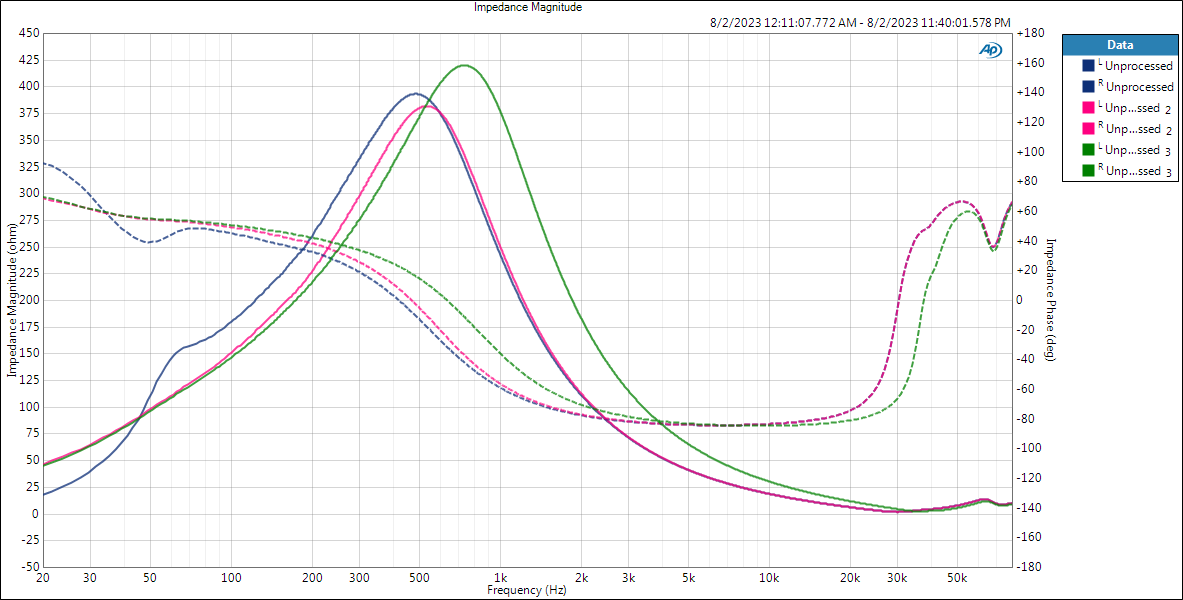
Here is the impedance plot (phase and magnitude) of the transformer in an SRD-7SB with the SB circuit disconnected. Three sweeps were run with 1V input, output open; 1V and 2V input, driving a Stax SR-404 with its bias supplied externally. Take an educated guess, which curve is from which test condition?
-
Output Stage Current Requirements for Electrostatic Headphone Amps
simmconn replied to JimL's topic in Do It Yourself
I see a few problems in your calculations. First, the load impedance is the characteristic of the phones, which is listed in your headphone’s spec sheet. It is not determined by the output voltage or current capabilities of an amp, which on the other hand are the amp’s design choices. Second, the reflected impedance to the amp is affected by many factors (and follows square of the turns ratio in an ideal case). In this case, the parasitics can have a significant effect on the load impedance the amp sees. Take a measurement and you may be surprised. Third, impedance is a vector. Using a scalar value is convenient but let’s not forget its vector nature and mostly reactive for the estat phones. The 1W of driving power would then be apparent power and not real power. Last but not least, may I suggest that we limit questions and comments regarding one project to a single or a couple of threads only? -
Building an energizer almost from scratch - advice on clamping zeners
simmconn replied to bobkatz's topic in Do It Yourself
That's all good statements in theory. My suggestion would be to plug-in the real-world numbers, do the math and find out what kind of voltage you really need/can afford, and go from there. For the protecting scheme, too. You now have a high voltage DC supply which can conveniently verify the protecting threshold of the candidate device. You could also connect the protection device/series resistor(s) to your phones and listen to them at comfortable levels. If you can't hear a difference, or even prefer the sound with the protection device present, viola! you've got a solution. FWIW, I found an MOV which looks like a 2W+ metal film resistor in my old Stax Lamba (normal bias). I guess at the time the non-linearity it brings was the lesser evil compared to a burnt driver. -
Building an energizer almost from scratch - advice on clamping zeners
simmconn replied to bobkatz's topic in Do It Yourself
An ideal shunt-type protection device for the estate phones should have: 1) Low (<10pf) and constant capacitance vs voltage and vs frequency - that pretty much crossed out all the silicon junction devices. 2) An I/V curve with a sharp corner, near-zero leakage within the operating voltage and well-controlled clamping voltage - that rules out most MOV devices 3) Fast acting. That excludes the gas-discharge type. What do we have left? Why use a shunt-type protector, just to give the amp and the transformer a jolt like a dead short when they are outputting close to their max voltage? The Stax transformer box adds a PTC in series with the transformer primary to mitigate this issue - and you know how people hated it. IMHO a better protection is to limit the output voltage of the amp. If the power rail voltage is limited, the amp's output is limited and the transformer's output is limited as well. -
Building an energizer almost from scratch - advice on clamping zeners
simmconn replied to bobkatz's topic in Do It Yourself
@bobkatzIMHO you are not likely going to get better performance with the TPA3116d2 class-D amp. It will have high noise and distortion than the amp modules in EHA5, plus the ultrasonic switching noise that may cause further intermodulation junk down the chain. Most if not all the imperfections you see in the measurement are caused by the transformer, such as higher THD at lower frequencies, the resonance at ultrasonic frequency that manifest itself as poor square wave response, plus other issues like phase shift (group delay distortion) that is not reflected in your tests. The transformer is the weakest link here, within the capability of the amp modules. Using a better transformer such as lundahl would help. I'm not sure if you can find one with turns ratio as high as 50. If not, you might want to switch to an amp with higher output voltage, if you need to maintain the 700Vrms output level. -
That's a common misconception about differential signals from signal integrity point of view. No output driver works out of vacuum. They are all power and ground referenced. Even with transformer isolation, there is imbalance in the windings and capacitive coupling between the primary and secondary, from windings to the core. In a practical world nothing is ideal. The AES diagram clearly shows how the current 'I' could create a noise voltage drop between the input shield point and the star ground point, which adds to the input signal in a common mode fashion. That's why there is a note in the end that says, 'as close as possible to each other'. How about at one single spot, can you get closer than that? Personally I wouldn't want to inject any dirty stuff from the ground of the source to IN- of my amp. So if I find out an RCA female to XLR male adapter connecting pin 3 to RCA signal ground while keeping pin 1 floating, I'd want to modify it.
-
Hmm, I wonder what kind of noise and hum level would be when you connect like that. Unless your source is true balanced pro gear with transformer-isolated output, most DACs and preamps have ground-referenced output stage. In other word, the +/- are not using each other as the return path, but pin 1 in that XLR cable. Once you include the PE connection and the signal ground connection in your common-mode return path, noise and hum inevitably gets included in the signal coming to the amp. Remember any amp has a finite common-mode rejection. However the theory says, I guess at the end of the day, whatever works best in my/your system matters the most.
-
I’m just saying, connecting like you described may not have the best hum rejection, and if we need to connect the PE and signal ground again at the amp chassis XLR input for better hum rejection, it defeats the purpose of running two grounds separately. That’s why I was asking if you have any measurement data to support your ground wiring scheme.
-
Ideally the PE connection doesn’t carry any supply current and is separate from the PSU return wire. However in the DIY T2 case, they are connected together in the PSU already. If you connect them again at the amp chassis XLR input (the amp PCB has a ground lug for that), it defeats the purpose of running them separately. Unlike connecting independently powered devices shown in your diagram, the T2 amp circuit is powered by the T2 PSU. So unless you have measured data to prove otherwise, I think using the PSU ground return wire(s) to the amp to double as PE should be sufficient. In my personal experience with DIY T2, the ground wiring is not a significant contributor to hum.
-
@jokerman777If the length of the spigot on the PPS washer gets close to, or is longer than the combined thickness of the TO220 tab and ceramic insulator, the hole on the L bracket must be large enough to let in the excess length. Otherwise the PPS washer would be crushed when you tighten the screw. Too bad you can’t do threaded holes on the L bracket for the same reason, and have to use the nut - split washer - flat washer combo which is a pain in the neck to work with when servicing the unit.
-
I agree that metal chassis should connect to the earth ground from the power cord/line input module. In general, I also connect the transformer electrostatic shield ground and the DC power supply ground (which is electrically connected to the amplifier's signal ground) to the chassis/earth ground. That seems to give me the lowest measured hum level. Sometimes grounding the input signal ground at the connector entry point to the chassis works best for me, but YMMV. In terms of DIY T2, since its in two separate chassis, the only way to ground the amp chassis is through the power supply ground wires in the umbilical cords. The center standoff near the back on the PSU board becomes the most convenient star-ground point. The wires going to the grounding point should be as short as possible and stay clear of the transformer leakage flux. Unfortunately that's not easy to do in the DIY T2 PSU chassis.
-
Both the 2SA1967 and the lessor 2SA1831 can still be had for less than $1 a piece, if you know where to look. They have the same B-C-E pin order so should be a drop-in replacement for the B832 (please don't take my word for it, verify yourself!). But I agree with you, it'd be better to save up for a better amp. On the Topping/transformer topic, I know people don't like the SRD-7SB because the transformers are taxed to provide the bias. Has anyone compared the SRD-7 and SRD-7SB with the bias circuit disconnected? I mean, does the additional bias tap on the SRD-7SB transformers hurt the performance even if not used?
-
Happy birthday, Kerry!🎂
-
The solder type is a lifesaver for DIYers, unless you want to deal with the uber-expensive crimper, the crimping dies, and the go/no go gauges. Having said that, I found the power rails considerably cleaner at the PSU board than at the amp board.