
simmconn
-
Posts
173 -
Joined
-
Last visited
-
Days Won
2
Content Type
Profiles
Forums
Events
Everything posted by simmconn
-
If the noise changes with the volume knob and appears when you turn on the source (not when you turn on the amp with no input signal), it sounds like your amp’s left channel has a problem and not your headphone. I would stop messing with the new phones and try a different pair of phones on the same amp and see what happens.
-
Sorry, wrong thread…
-
Since many of us would never be able to afford one, might as well take a guess what’s in it. A Megatron with SS CCS and 12AU7 cathode followers driving the DHT final stage?
-
Background noise from headamp aristaeus
simmconn replied to qqiao's topic in Headphone Amplification
@qqiaothere are a quite few posts in the DIY forum of this site talking about estat amp grounding that you can use for reference. Basically I’ve learned the following: 1. The metal chassis should be connected to the protective ground on the AC power inlet. This is for safety, as well as a good starting point for a hum-free amp. 2. There are two types of ground on the volume pot, the signal ground and the metal frame/shaft ground. I would keep the signal ground running along with the input cables’ signal flow, and connect the metal frame ground to the chassis (usually by tightening the collar nut with a tooth lock washer is sufficient). 3. power-line induced noise can have a few different sources, such as due to different ground AC potentials between the source and the amp; due to the power transformer leakage flux flowing thru a closed signal or ground loop; or in tube amps, the leakage flux directly modulating the signal current in the tube. The common wisdom calls for single-point grounding, either at the power filter cap, or at the audio input jack. Note that the left and right audio cables can also create a ground loop, so it makes sense to run them closely to each other inside the enclosure. 4. Some units provide a “ground lift” feature, which gives the option to connect the electrical ground to the earth ground thru an RC in parallel as opposed to direct connection. I haven’t had personal experience where ground lift is especially useful. Within the amp, everything is relative to the amp ground. The ground only becomes dirty when there is dirty current flowing from one grounding point to another. Your job is to find that current and get it out of your ground. -
I wonder what’s in those black boxes marked ‘phase splitter’, 1:1 transformers? I see 4 coax cables going into them.
-
TL; DR: I’ve wanted to build a Blue Hawaii ever since I read about it on head-wize. I finally got around building a mini BH-BJT packed into a small enclosure like a can of sardines. Many small tweaks were done in attempt to reach the measured performance of the original Blue Hawaii. The details of the journey are recorded here. Many thanks to Dr. Kevin Gilmore for designing this legendary project. Thanks to Kerry, JimL, Joamat and many others for making it such a fun journey. KGBH1.pdf

- 242 replies
-
- 15
-

-
goldenreference low voltage power supply
simmconn replied to kevin gilmore's topic in Do It Yourself
@dip16ampthe test results are all relative (in dB). Are you sure the 0dB reference is calibrated to 1V rms when you interpret -120dB as -120dBV? Even the most advanced Audio Precision APX555B is “only” spec’d at -117dB of range plus 1uV. Besides, the limited bandwidth of the line matching transformer and the high-ish 10k resistor in combination with the input capacitance of the ADC probably make the test result look quite a bit better than it actually is. -
Static-like Sound Coming from Left Channel?
simmconn replied to ThePhoenix's topic in Headphone Amplification
Where are you located? We have forum members around the world, and someone close to you maybe able to help. Although the circuit is not complex, troubleshooting intermittent noise problems often require a lot of patience and decent test equipment. -
PBHV2160Z is nice due to its high HFE and low Cob. I'll be using PBHV2160Z and PBHV3160Z in my upcoming GRHV build with off-board e-caps. From simulations using those transistors I learned that C5 needs to be increased to 15pf to 22pf for best phase margin, and 47n is still the preferred value for C4 that provides a low and consistent output impedance across the audio frequency range. Another interesting find is that the circuit needs about 100uF output capacitance to be stable, and increasing the value of that cap has a diminishing return in the performance, unless the cap has really low ESR (such as film caps). In case the cap's ESR is high, some additional compensation can be added to ensure stability (hundreds of pf across R7). The above findings are for the original GRHV with 400V output. YMMV if the output voltage changes.
-
@JoaMat Did you measure the removed part and see which transistor and which junction failed? If it takes a while to fail, chances are the power dissipation is over spec. Something else could be leaking that causes excessive current through the part. An IR camera would be handy in troubleshooting problems like this. The STN0214 may have a different Cob than the original part KSC5026, and the closed loop gain of the regulator is also different (20x vs 40x), the compensation capacitor values may need to be adjusted to maintain stability.
-
Yes that’s what I would do.
-
The SiC did survive and still tested good all the way to 1700V on a curve tracer. I guess the ST9360 had a slow death and the BC557s gave up before more current could damage the SiC.
-
I’ve been using the DN2540 in TO-92 package since my first Carbon build without any problems on the amp board. However I’ve seen two instances where the DN2540 on the GRHV developed a Drain-to-gate leakage. That caused excess current thru the HV PNP. In one case (my own build) it was caught in time and didn’t do any real damage, in the other case (someone else’s board with a TO220 DN2540) the PCB was cooked, the ST9360 failed and brought down both the BC557s. The leakage problem is regardless of the DN2540 package. I’m suspecting in the cascode CCS there may be a corner case where it is stressed beyond the safe limit.
-
The GRHV is not particularly fault-tolerant. If any of the high-voltage part had a breakdown, it will likely cause a chain reaction and bring down other parts, including the expensive (if you didn’t buy from AliExpress) LT1021. So being able to test the breakdown voltage of the parts before putting them on the board helps a lot.
-
It would probably work, but I wouldn't call it a 'good' replacement. You would have to deal with a different package, higher Cob and lower Hfe. In theory any NPN with sufficient breakdown voltage can be used in that position, but since it is the only gain stage in the regulator (both the STN9360 and the SiC FET are followers) and consumes very little power, I tend to use lower current parts with potentially higher Hfe. The compensation cap value was designed for the KSC5026M, so if the replacement part has lower Cob, increasing that cap may be necessary for the stability of the circuit.
-
What’s the purpose of the 555? It seems that it’s not doing much meaningful. Even if you want to keep it, at least its pin 3 and pin 7 output opposite polarities such that you won’t need another inverting stage outside…
-
Thank you, and big thanks to @kevin gilmore@Kerry and many others who made this DIY journey really enjoyable!
-
Thanks! I've got to bump this thread to page one with some real stuff 😀. The GGPT (Grounded-Grid Pentode/Tetrode) now gets a proper PCB laid out: I made a few deviations to the common choice of parts: 1) I found some 2SK332, could be Sanyo's answer to the low noise dual N-JFET market back in the day. They cost me about 60 cents a pop, so I ditched the LSK389. The footprint is also usable for a pair of 2SK170s. SOT-23 footprints are added for the 2SK209, and a few others that share the same pinout. 2) Through-holes on the SMD pad for the SOT223s are a big no-no for machine assembly due to solder wicking, but works okay for hand soldering. It allows the use of A970/C2240s. I found some from a Chinese manufacturer Foshan Blue Rocket Electronics, pretty decent build quality, good low-current linearity, and cheap (14 cents a pair). 3) All through-hole RCs. I know the world has moved to SMD but I have quite some through-hole resistors accumulated over the years, and personally prefer leaded components on tube PCBs due to the thermal and mechanical stress they have to endure. The FU50 tube sockets are so big and everything else have to dance around them. I chose not to use slotted pads at the exact socket pin locations, instead having soldering pads on the side allows flexible or semi-rigid connections from PCB to the tube socket contacts, which can absorb the strains. The scheme is similar to what Stax had on the original T2 PCB. A couple more mounting holes are added to allow other types of tube sockets to be used. The board mounting holes have the same distance compared to the Carbon board. This board can overlay on top of the Carbon board in the chassis where I have enough Z space left. They can share the heat sink and the power supplies. The goal is to be able to switch between them with a flip of a switch. The GG Pentode with GU-50s and the GG Tetrode with 807s, side by side: The 807s have slightly better measured performance, at the voltage level that I probably never going to drive my phones at (when I'm wearing them).
- 14 replies
-
- 12
-
-
The so-called 'active battery' is a shunt regulator IMHO. I would recommend that you simulate any circuit changes for performance (shunt impedance) and stability. The original circuit does not seem to have enough phase margin and can use some compensation. My calculation shows either adding a 1.2pf cap across the two 820k feedback resistors, or increasing the shunt capacitance to 0.1uF would help. They each have their pros and cons. The calculated capacitance is so small that parasitics can throw the circuit in either way and make it 'touchy'. Using 2.2nF compensation cap would significantly increase the loop gain in the mid- to high-audio frequency range and reduce the output impedance as you have observed, but also make the stability worse. Since the active battery is part of the signal chain, I would rather shoot for flat impedance across the audio range and as small phase shift (group delay) as possible. I'm not sure what your test gig looks like. It would be important to test it with a source impedance similar to the real circuit. My sim tells me that the original circuit when properly compensated can be pretty flat within 20KHz and has -3dB point over 200KHz. On the other hand, the LT1021 due to its high-ish operating current requirement, does not necessarily bring much gain to the overall performance of the active battery compared to the LED strings.
-
Ah, okay. Sorry I misunderstood the question. It’s certainly possible, but usually the two CCS blobs are physically away from each other. IMHO given the other potential component mismatches, sharing the same LED string may not make a big difference in the current matching between the CCS.
-
My take is that 2 LEDs in the string allows a higher emitter resistor value and therefore better local NFB. Sim shows that the effective impedance of the CCS roughly doubles with 2 LEDs vs 1. That come at a cost of reduced voltage compliance range and slightly increased power consumption. They are not a big deal for high voltage CCS, though.
-
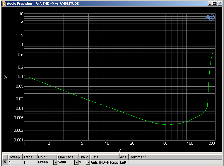
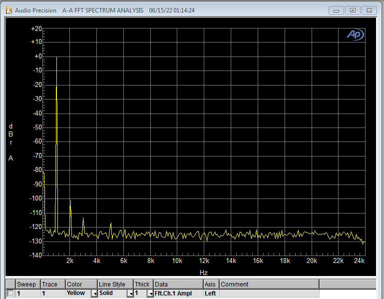
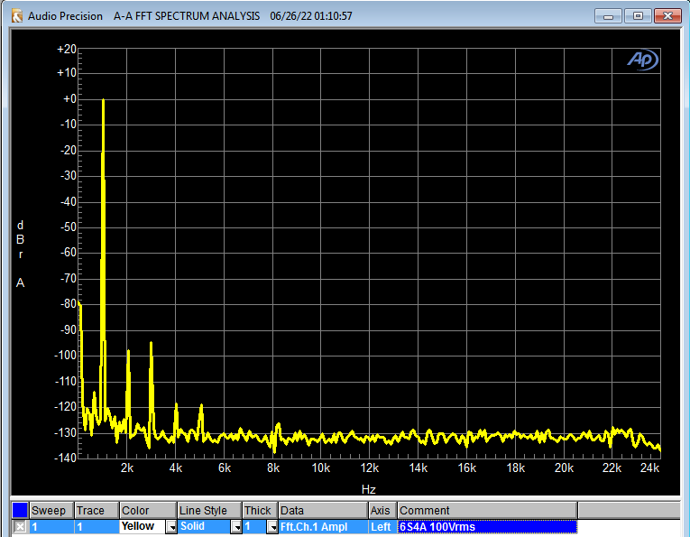
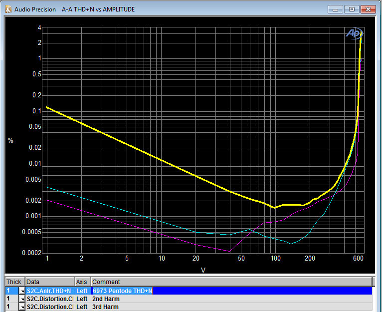
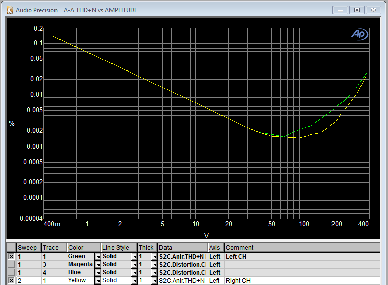
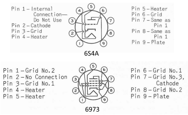
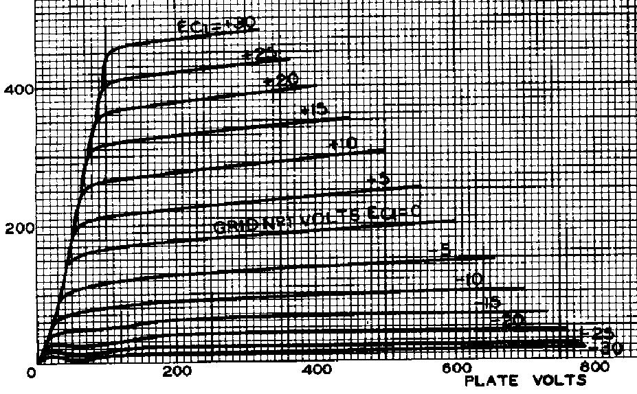
Although the KGST uses the same front-end as BH and Carbon, its simplicity comes at a cost. In the 'stock' form, the open loop gain is about 78dB and closed loop gain about 59dB. Having only moderate global NFB means that the circuit has to have a wider open loop bandwidth and good linearity to begin with. It also suggests that the measured performance would depend a lot on the matching and inherent linearity of the tubes. Below is the THD+N vs amplitude plot I did earlier on the 'stock' circuit. The max output is about 200V. It kind of falls short for an amp with ±400V supply. With the experience from the pentode experiment on Carbon, I tried a few pentodes and tetrodes with the 'stock' circuit. The first one I tried was the 6973. Why 6973? Because it's pinout is very close to the 6S4A, such that I didn't even need to cut any PCB trace in order to use it. The result was quite ok. The max output went up to 500V and the lowest THD reduced by about a half. Knowing how much the 6973 costs on ebay I think I should have a better use for them 😉 Then I tried a few others, including the 832A. It has one of the cutest bottles and yet is not that expensive. I was eyeing on the Breeze audio 832A SE amp enclosure. The box may look hideous to some people, it would be really cool to have a unique eStat amp like that - if still offers reasonably good performance. The 832A didn't pan out very well. The THD flattened out at 0.01%-ish, mostly 2nd harmonic, due to the mismatch between the two tetrode sections. Some people may appreciate the 'tuby' sound, I decided to move on. I looked for a triode with amplification factor of 30 (twice that of the 6S4A), which also allows 400V DC on the plate (800V peak). It's not that easy to find real triodes like that, unless I go with the exotics such as the 801-A/10Y. I heard about the 12HL7/12HG7/12GN7 family. The video output pentodes designed for the color TVs in the late 1960's. They allow 400V on the plate, have a mu of 30 to 50 when triode-strapped, and said to have great linearity. Below curve was captured with one of them at X=100V/div, Y=5mA/Div, Vg1= 2V/step It turns out (again) it's not easy to find well-matched pairs because the curves in the high voltage region vary a lot from tube to tube, and the g2 power would be over spec when triode strapped idling at about 400V. I did get some nice distortion plots when they are wired in pentode mode (below FFT with 12HL7 at 100Vrms output). Unfortunately not all of them are happy with 800V peak on the plate, although 400VDC is okay on paper. So I came back to the drawing board, trying to make it work with the 6S4A. In the 'stock' circuit, the limiting factor to the output swing is the signal amplitude at the 6S4A grids. Adjusting the ratio between the 200K/6.8K resistors on the active loading NPN pair can increase the idling voltage and improve the max swing into the 6S4A. The downside is that the output impedance of the driver stage will increase, and the open loop bandwidth drops a bit due to the Miller caps on the 6S4A. Also I don't need the full 60dB gain. '200mV sensitivity for rated output' was established from the analog-era when tuners and tape decks are the most popular sources, not to mention 100mV for rated output. Doubling the resistors at the source of the input JFET aught to do it. The end result is extended output swing: And a not super clean, but still okay output FFT spectrum at 100Vrms. Well, that seems to be the best I can do. I'd live with(in) its limitations, close the lid and enjoy the music!
-
I took the challenge again to squeeze a DIY eStat amp into a small enclosure. This time is a KGST in a Breeze Audio 2409. I was using an Antek AS-1T350 with a separate low-profile quasi-toriod for the LV supply. The Antek was well shielded with both copper and steel bands under the wrapping, I still need to move it all the way back to reduce the hum. I'm glad I pulled the trigger and ordered the custom R-core transformer. I asked the vendor to build two identical bobbins to balance the flux, each with a 115V primary, a 350V, a 17V and a 6.3V secondaries. With the copper band on the outside, the flux leakage is so low that I couldn't pick up anything significant at 60Hz or 120Hz on the FFT. I have more than twenty 6S4 and 6S4As, many of which are NOS. However I had a hard time matching a second pair, and had to decide between a well matched pair that is slight noisy and one that's less well matched. The curves look all similar below 400V, but could go all over the place on the higher voltage region. The below picture is kind of an extreme case, an example that two tubes both testing good on a tube tester at 150V on the plate, may be quite different when you need them to swing up to 800V: <To be continued..>
-
You’ll need some kind of +/-15V power supply, GRLV being an option. There are left and right versions of the GRHV board, one with the bias supply and the other with the 7815/7915 LV supply. The sellers from China cut the corner and only produce the GRHV board with the bias supply. You’ll end up receiving two of those, and still need the LV supply.
-
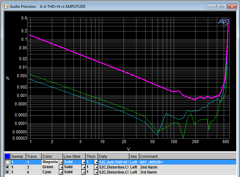
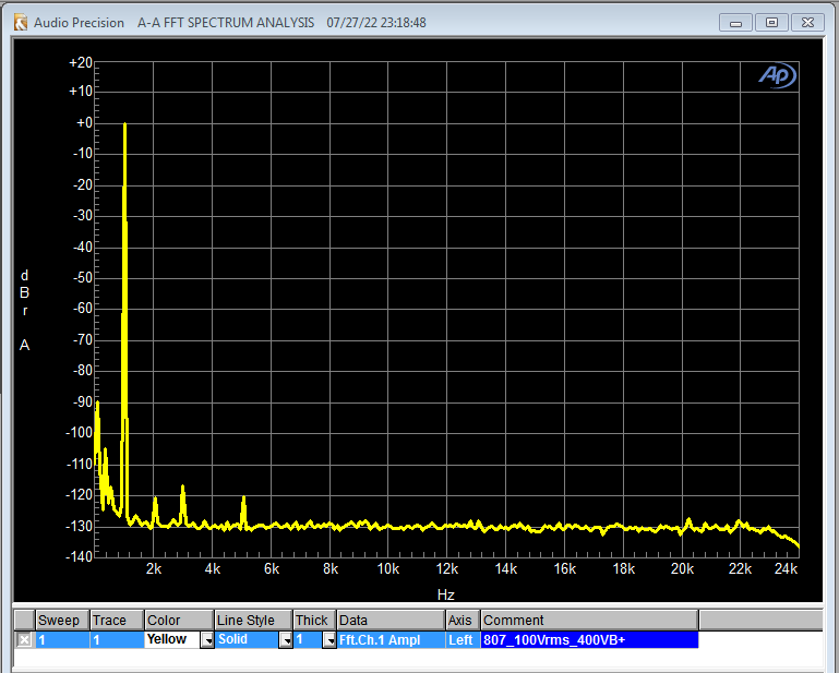
The pentode experiment gets a little twist - with a beam tetrode. In my search for an acceptable output device, I went through the popular low-power transmitting tubes. The 807/6L6 family has such a wide, kinky curve in the low current region with typical Vg2 (250V) and was rejected as a candidate at the first glance. However, the curves around zero Vg1 looks quite linear. Lowering the Vg2 could sort of 'bring them down' to the low current region. With about 60V on the G2, the kinks are largely gone, and the linearity looks pretty good (pictured below X= 100V/div, Y= 5mA/div, Vg1= 0.5V/step). Another benefit is that Ig2 comes down considerably with such a low Vg2, which allows me to use the same simple G2 supply used with the GU-50 (zener diode paralleled with a 10uF cap). I compared quite a few tubes on the curve tracer. The National Union 807s (shown above) from WWII era seem to have the best linearity and are the most stable. The RCA and Sylvania tend to oscillate on my test jig. 1625s are about the same. Unfortunately I don't have enough National Union for a matched quad. The earlier 6L6/6L6-G are not officially rated for 400V plate voltage and have to be excluded. The Tung-sol 6L6WGB/5881 (the real deal, not the 'reissue') looks much more linear compared to the 6L6GC. The Sylvania 5881 (shown above) although has the same internal structure as the Tung-sol, doesn't seem to be as linear. The 1624 would be an interesting direct-heating variant that has a bit higher gain than the 807. The 2E26/2E24 brothers are suitable, too. Here are the 807s on the test bed: The result is convincing: The 100Vrms output FFT shows harmonics -115dB below the fundamental: The 1624 turned out to be a disaster. It was hard to get a clean, low capacitance filament supply. When attached to the signal path, the common-mode noise would kill the S/N and the capacitance would mess up the frequency response and THD. I have to admit I don't have much experience with direct-heating tubes in circuits where every uV counts. It would be nice if the few exotic direct-heating tube eStat amp owners can get their units measured and share their secret to success... The grounded-grid cascode output stage is such a nice thing that it allows us to play with many tube types, as long as they have enough plate voltage and power ratings and are reasonably linear. We could end up having unique amps that still have top-notch performance.
.jpg.3be03c3a74da4ef29002b73755c04827.jpg)
.jpg.d41660e97a65cdad7e56a62fc76e39ae.jpg)
.jpg.ecc1c2cd21427d8c799091f0c545edaa.jpg)
.jpg.d475321966f5769f0d3a3f0482762ecd.jpg)
.jpg.1c9302670ba81f1b17c9c16954fec866.jpg)
.jpg.6ec3f0fd7c77c52300c17f3f595a4acd.jpg)

.jpg.fce1991dc322ef72d687ba06df701c5e.jpg)
.jpg.9673bed850c4915aeacee856d6255850.jpg)