
simmconn
-
Posts
173 -
Joined
-
Last visited
-
Days Won
2
Content Type
Profiles
Forums
Events
Everything posted by simmconn
-
As planned, the other channel is modified the similar way but with GU-50 tubes as the output device. The performance is comparable to the SiC FET: The distortion profile at 100Vrms output is pretty good, too, with all harmonics -115dB below fundamental. It turns out, the ESL speakers require considerably more voltage than 1KVrms. My Martin Logan CLS-II transformers have about 1:160 step-up ratio at the low end, gradually tapered down at the high frequencies - so some EQ is also needed for a direct-drive amp. The Quad ESL-63 is said to have 1:260 step-up ratio. 1KV is probably just going to make it to a BGM sound level...

-
hmm, perhaps someone has the habit of populating all the parts first, and then finish up all the soldering joints. Easy to miss a thing or two when there is no AOI. After all it’s only the servo…
-
Share your favorite stores and parts here.
simmconn replied to omendelovitz's topic in Do It Yourself
The local surplus store is closing its doors next month. To not let the 2SC3381s go into a black hole, I’m running a group buy. Mixed GR and BL grades, $0.5 each with minimum of 10 pcs. Shipped from California. PM me if interested. Also available 2SC3067 dual NPN at the same price. Sorry no JFETs or high voltage transistors. Group buy closes Friday 6/24. There is a chance someone may scoop them up before I do, in which case refund will be issued. Please don’t blame me if that happens. -
Based on your first question you should probably stick with the original design. The 24V zener diode protects the MOSFET from excessive Vgs during power up, when the output capacitor is charged up from zero. Since you recognized the CCS, I probably don’t have to elaborate the benefit of a CCS vs a resistor. The simple answer is yes, you can replace the CCS with a resistor with reduced performance. The 10M90S is in short supply, at least from the US distributors. You can replace it with IXTP01N100D, or based on your rectified DC voltage, try a DN2450 or DN2470. The 1.2k resistor would need to be adjusted to obtain the same current through the zener diode chain as with the 10M90S.
-
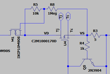
Thanks. A fixed-setting current limiter before the passing device would also help the SOA issue. I can also do something like the following: With carefully selected R5 and R8 values, M1 and U4 can split the start up VIN. A resistor can be added to the M1 source so it also acts as a current limiter during normal operation. After all, most of the high voltage Si-MOSFET and SiC FET are designed for switching applications. We need to tread carefully when using them in linear mode.
-
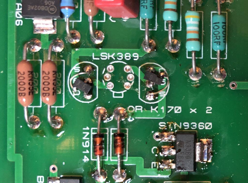
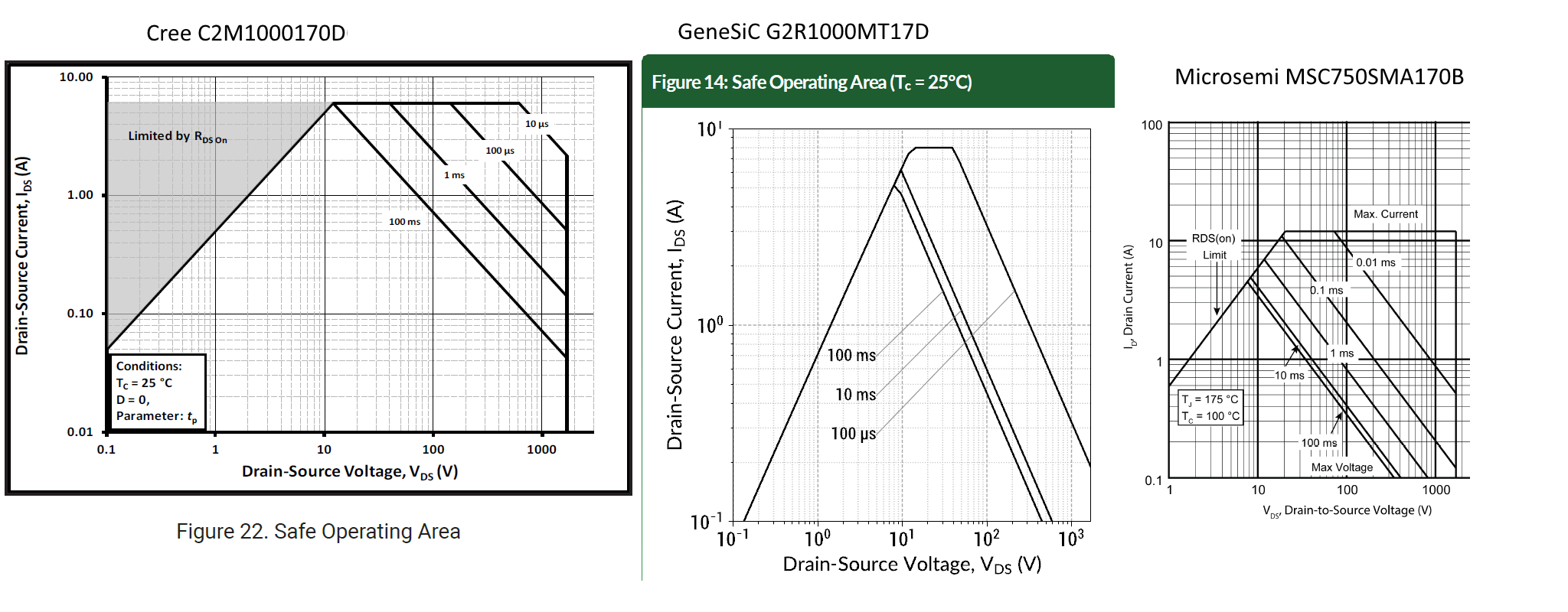
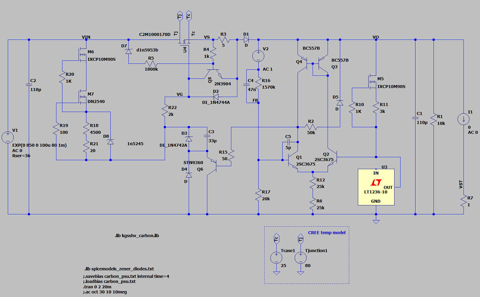
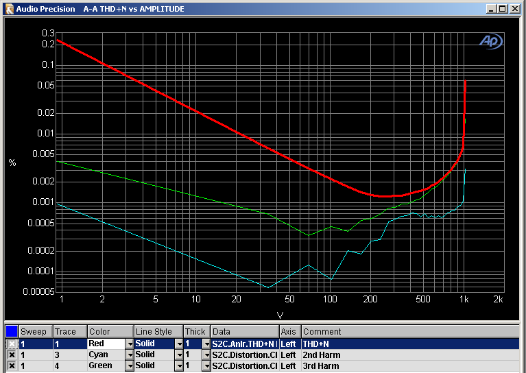
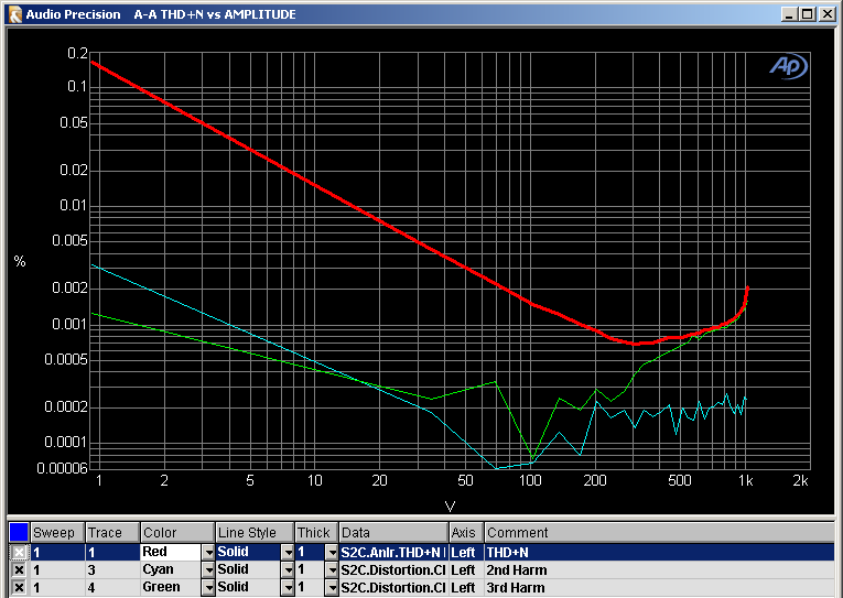
The second part of the experiment is the PSU. The Circlotron HV power supply (goldenreferencehv900new.pdf) uses an ingenious way to overcome the component voltage rating limitations, by using a floating reference point at 1/2 of the output. Since I'm not pursuing 900V, maybe I can get away with replacing a few parts in the GRHV and settle at 800V? Aside from doubling up on the input and output caps, the STN9360 needs to be replaced with 2SA1968, and KSC5026 replaced with 2SC3675 or 2SC4686A, and the resistor divider updated. Done, I thought. After a couple of minor volcano eruptions, I had to go back to the drawing board. Since they both failed at power up, it looks like either the current limiter didn't work, or it was overwhelmed because the SiC-FET had a D-G breakdown. I put the SOAs of the SiC-FET side by side, comparing their allowed VDS under 0.1A of current at 25C, which is the PSU start up condition: Apparently the C2M1000170D is the most robust, allowing 700V (100ms). The G2R1000MT17D scores the second, allowing about 450V. The MSC750SMA170B only allows a little above 300V. Considering it's specified at max Tj, the 25C spec should be better. So what works for the C2M1000170D may not work for the cheaper subs. It could be SOA violations that killed the SiC FETs. The GRHV soft start uses the cascode CCS to charge the Tantalum cap until the SiC FET VGS is higher than its threshold voltage. The SiC FET turns on slowly so the current limiter has plenty of time to get in action. The output cap is then charged with 0.1A of current over a few seconds until the preset output voltage is reached. The above assumes that the PNP is ON at the beginning, which is not exactly the case. The output cap needs to be 'pre-charged' to about 1.2V to establish a DC path for the PNP to turn on. The per-charging is done with the SiC FET fully on, and only the current limiter in effect, when the SiC FET is most vulnerable. Although the pre-charge time is short (several ms depending on the output cap), it's better safe than sorry. My solution is to add a diode D5 to establish an initial DC path for the PNP. I chose a low-capacitance small signal schottky diode, with a resistor R2 in series to further reduce the effect of its junction capacitance. Also during the soft start, the charging current increases quickly to reach the current limit, but the output voltage only ramps up linearly, which means the SiC FET would pass a lot of current when its VDS is still high. It would be great if the VDS can affect the current limit and set it lower during ramp up. So I added R5 and zener D7. D7 has a higher voltage than the normal working dropout voltage, so R5 wouldn't take effect during normal operation. After the above mods, the SiC FET has not failed. I also reduced the output voltage to 750V and reduced the input accordingly. The last failure happened a few minutes after turning on, and was caused by thermal runaway of the PNP. It turns out the DN2540 developed some kind of gate leakage, where the voltage drop on its source resistor no longer controls/represents the output current of the CCS. A lot more current gets dumped to the PNP, causing it to burn. I couldn't figure out what caused the damage, perhaps some transient conditions. So I added another zener diode D8 to protect the DN2540. Now both GRHV PSUs are upgraded to 750V output and work stably so far. The amp boards work okay when connected to the 750V PSU. Now is the time for some measurements. First is the all-JFET configuration. And swapping the SiC FET back in as the output device, with visible improvements: The SNR is about 6dB worse compared to the original Carbon under 400V PSU, due to the feedback resistor mod in order to get a higher output voltage. Did I get the 1kVrms output I was looking for? Yes. Well, sort of. The problem is, the volcano eruptions ruined two SiC FETs and I don't have any more to populate the other channel. Digi-key has the C2M1000170D back in stock now, but the price has gone up to nearly $10 a piece. I guess I'll keep using the GU-50s on the other channel.
-
I was going to name it 'Double the Carbon, double the voltage, double the fun', but I'm afraid that would be too wordy. Ever since I measured the output swing capability of the Carbon, I wanted to see if it can drive my ESL speakers. To do that, I'd need a beefed-up version that can output at least 1kVrms before clipping. That's 1414V peak, out of a ±750V to ±800V PSU. To simply scale up the Carbon amp and the GRHV PSU without major changes to the PCBs, a few hurdles would have to be overcome. First is the 900-V rated 10M90s in the cascode CCS that bottom out with ±450V PSU. When I was browsing the high voltage FETs at Mouser, I found the UnitedSiC UF3N170400B. It's a 1700V 6.8A SiC JFET, naturally in depletion mode, perfect for the upper device in the cascode CCS. The threshold is about 9V, which helps the DN2540 to get further into the constant current region yet keeps the power dissipation still in check (no heat sink needed even with the TO-92 package). The drawback is the package. The TO268-7 isn't too friendly for a DIY thermal solution. I had a few carrier boards made with aluminum-based PCB. According to simulation, the little board would give me 9 degree temperature difference from the package case to bottom of the board when the FET is dissipating 9W. I chose black solder mask, hoping to get a bit better heat radiation capability. 10 boards cost me about $3 at JLC. They also have copper-based PCB with a special process to have the base copper flush with the top surface for a much, much higher K. Too bad the NRE is about $150, so I chose the cheaper route with aluminum. The insulation is good to 3kV so this board can be bolted directly on the main heat sink without additional insulation. Isn't that great? The next bottleneck is the 600-V rated STN9360 when the PSU voltage reaches ±600V. I replaced them with the 900-V rated 2SA1968s. Thanks to the cautionary words from spritzer, I started cleaning up traces with high voltage differential that are getting too close to each other. I removed the middle pad 'A' in the 10M90s footprint, and re-wired a couple of traces on the back. With the bias changed from 24V to 13V above B-, the JFET can be used as the output device as well. At almost $10 a pop, they are considerably more expensive than the SiC MOSFET they are replacing. So the full-JFET configuration shown below is more of a proof-of-concept than anything else. The feedback dividers are changed from 200k:200 ohm to 440K:470 Ohm to maintain the gain and allow the output swing to double, without having the feedback current overtaking the idle current through the input JFET. Two 10pf 1KV caps are in series as a 5pf cap, since I don't have the proper 2kV rated caps. Not a great idea. I was lucky it didn't blow up. Technically the board is now ready for up to ±850V. I tested the SiC-JFET 'doubled carbon' config with ±400V PSU. The performance is slightly worse than the original Carbon. Is it worth the effort? We'll see. (To be continued...)
- 10 replies
-
- 13
-

-
@ibuski It looks like an used USSR-style socket. I would prefer that type of socket more than the NOS socket from China. I don't think the variations in design matter that much. As long as they were originally made for the military/industrial use, the quality should be trustworthy. @nopants The 10M90s still burn 7 to 9W each depending on the B+ voltage and the idle current. Using the enclosure side panel as heat sink should be doable, but it could get pretty hot. I would put some warning sign stickers on the chassis.
-
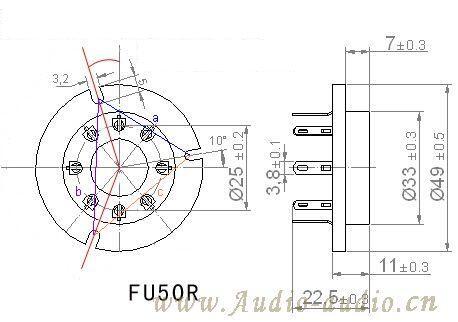
@ibuski Thanks! Speaking of low-cost FU50 sockets from China, there are different kinds. The socket on the left was removed from a NOS socket set with the cast aluminum frame. The frame helps the tube to align properly, and also works as a mechanical shield of some sort. It is unnecessary for a DIY amp IMHO. The ceramic socket base is pretty well made with good tolerance. The pin contacts have large flared openings and two holes on the soldering tab. The entire socket set including the aluminum frame can be had for about $3 each in the Chinese domestic market. The one on the right is the 'new production'. I got them for less than $1 a piece. Some with tin-plated contacts can be even cheaper. However the contact has a much smaller opening on the top, and a single oblong hole on the soldering tab. There is a risk of pins getting plugged into the well but outside the contact. The ceramic base are often poorly made with an uneven mounting surface. What's more, the pin 1 location is different from the NOS socket. Do not mix them! I would say go get the NOS socket set, spend a few minutes to remove the frame and end up with a socket in better quality. The socket mounting hole pattern is somewhat unique. A caliper and some middle-school trigonometry will be useful to figure out the exact angles of those mounting holes.
-
Since you are getting so close to the Paltauf and understand how the circuit works, why don’t you share with us the details? There is no problem for an unaffiliated user to disclose what he/she can see in plain sight, I assume. What I can see is that sharing is part of the core spirit of this site and what drew us together to begin with.
-
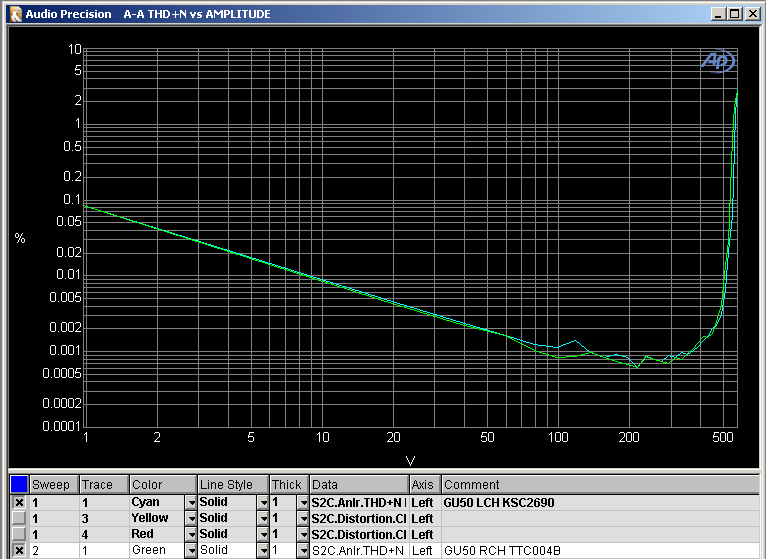
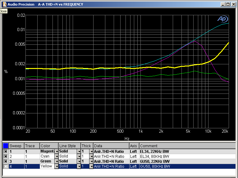
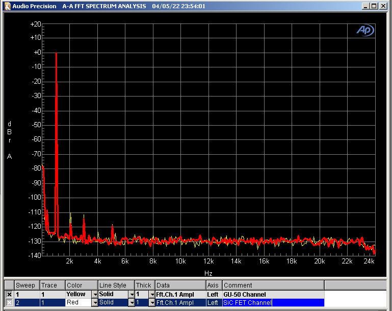
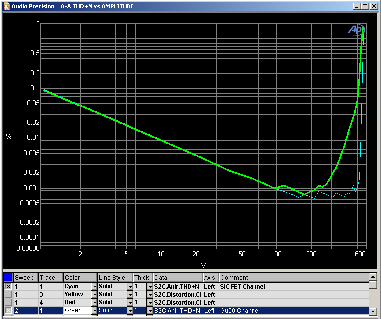
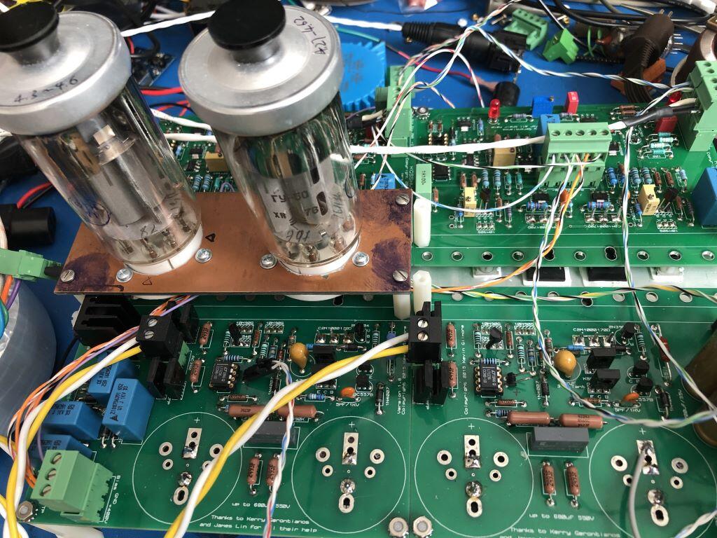
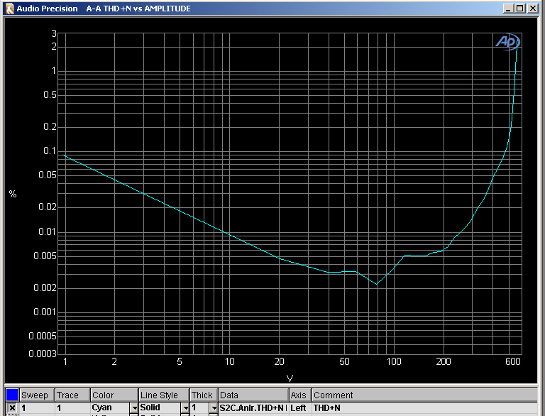
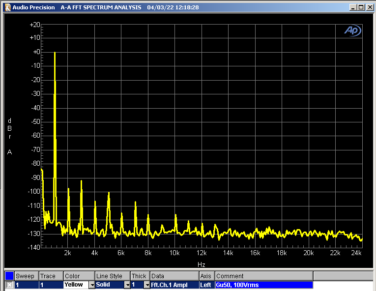
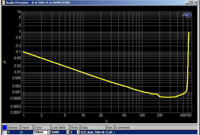
I'm finally able to put a closure on this pentode experiment, sorta. What finally improved the THD figure between 300V and 500Vrms output is the driver transistor. I replaced the PZTA42s with TTC004Bs when trying the original GG circuit with EL34s, while the PZTA42s remained in the left channel. With SiC FET as the output device, the driver transistor has a pretty steep load line, so the nonlinearities on the upper left portion of the curve didn't matter that much, as long as the idle Vce is chosen to be high enough to avoid that area. With the GU50 tube as output device, the driver transistors not only need to swing current, but also swing voltage (about 10Vpp), so the load line is more flat. The nonlinearities of the transistor becomes more problematic. The PZTA42s have to go. The KSC2690s I have on the left channel have higher hFE than the TTC004B on the right. The two channels ended up having very close THD+N curves. The 2nd harmonic is more prominent than the 3rd in the left channel with the KSC2690s, not sure if that's consequential. The hum is 110dB below the 100Vrms mark, with the 12.6V filament transformer CT simply tied to B-. I'm quite happy with the sound on my SR-009. It has the basic characteristics of the Carbon with a very slight touch of tube softness, yet not losing resolution or immediacy. I searched up and down but didn't find another pentode more suitable for this role, at least on paper. If some day I manage to put this into an enclosure, the ugly 'hats' would surely be sticking out.
-
Thank you, Dr. Gilmore. Given the background of amir (mid-high level on the corp ladder at M$), I wouldn't expect him to be as hands-on as the lab monkeys who spend most of their days with an AP. In an earlier post on that site I saw him struggling with setting up the AP to measure the deviation from RIAA of a phono pre-amp. Apparently he's never done that before and just like many of us, don't want to read the manual. Everyone has his/her limitations and comfort zones that takes some courage and effort to step out of. To give this guy some credit, he is able to measure the conventional gears in a consistent way, disclose the data and offer some objective comparisons/analysis, at no cost to everyone who is interested. That alone is worth some praise. Besides, some data is better than no data. When it comes to discrete R2R DAC, what intrigues me is that most designs use generic logic chips to drive the resistors. No matter how well the resistors are matched, the driver chips are not. No manufactures would specify or production-test the matching of a 10 cent bus driver, bit-to-bit or part-to-part. Parts coming from the same batch could be from the same wafer and perform somewhat close to each other, but there is no guarantee. The end result is therefore pretty much on a 'best of luck' basis.
-
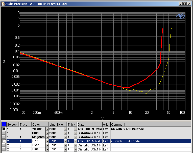
While waiting for the GU-50 sockets, I found a pair of reasonably matched EL34s, and decided to wire them in the original GG circuit for comparison. The TTC004Bs are used as drivers. Above the THD+N curve turning point at around 80V (multiply the X axis by 10 for actual voltage), the majority of distortion is 3rd harmonic. So I think the tube matching is not the major contributing factor here. The EL34 is biased at -37V, which means the driver transistors have to work really hard to push the tubes to make the output swing. The Pentode could be a better choice in a simple circuit such as the Grounded Grid. A more complex BH-style final stage would be needed to make the EL34 really shine. The triode-connected EL34 also lost on the high frequency distortion (100Vrms)
-
Thanks for the info! It is definitely helpful when I experiment with higher supply voltage next. I'll probably mill away some copper and apply some high voltage RTVs.
-
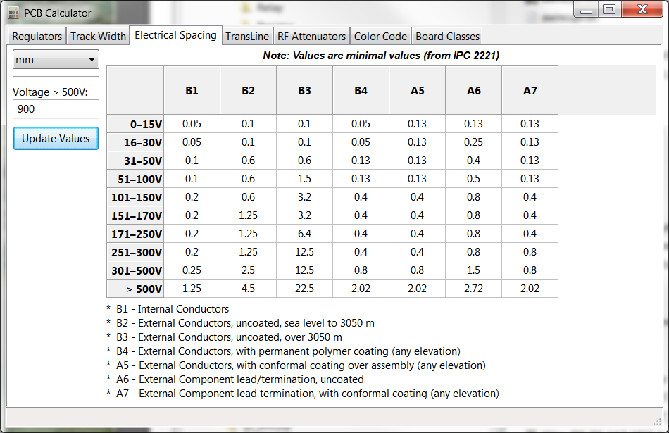
I stumbled across the Electrical Spacing section of the PCB calculator in KiCAD, which is from IPC2221A, Generic Standard on Printed Board Design. According to IPC2221A, most of our high voltage e-stat amp PCB build will fall into the B4 and A6 case. It looks like we may have a problem with the clearance. The biggest problem is with the IXCP10M90S footprint, where the conductor-conductor spacing is only 0.5mm. The SiC FET footprint is better at 1.7mm. Some minor problems here and there where the spacing between B- and other nets are about 0.5mm. I don't think anyone is conformal-coating the board after assembly. So in order to be fully compliant, especially for the (semi) commercial builders, it would be better to revise the PCB.
-
For the same phone, the lower the secondary winding impedance tap you connect to, the lower the output and the lower the distortion (assuming class A SE output stage). The max power transfer happens when you have a matched impedance. It’s not recommended to connect to a tap that has higher impedance than the load.
-
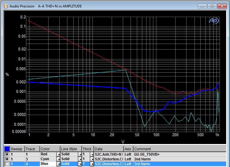
Now we are talk'in 😉. The tube channel has become really close to the SiC FET channel, both at 100V output. The performance is not yet at the Carbon level, but is pretty good for a tube amp. What was the problem with the previous mod? The simplified G2 supply didn't work well. This tube is quite sensitive to Vg2 (which may make it a good candidate for G2-drive applications, given the low Ig2). The previous circuit has Vg1 as part of Vg2, so the Vg1 variations causes Vg2 changes. The solution is to use one 150V zener diode for each tube, put it across G2 and K, and feed <1mA of current from GND using a resistor or a current source. I also added a 10uF capacitor in parallel with the zener. Without it, the output clips at around 300V but the distortion still looks good before the clipping. Now the circuit should deserve an audition. Since the main problem is the knee on the Ia curve and Ig2 curve below Va=100V, with higher B- (500V maybe?) and perhaps higher current, the tube circuit should perform even better. I'll leave that to the next episode. For now I'm waiting for the sockets from China to build the other channel.
-
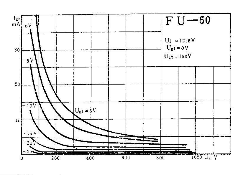
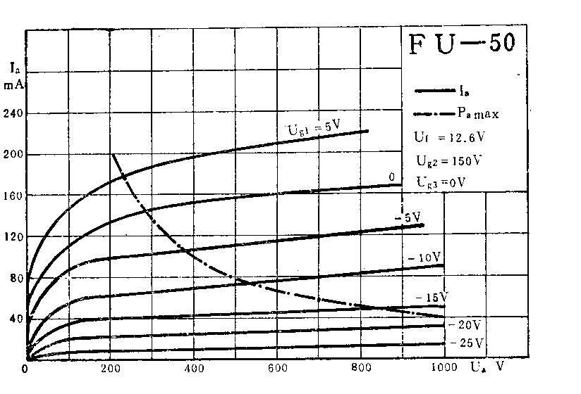
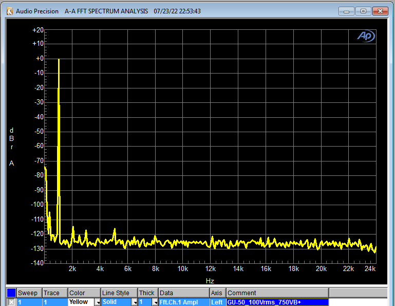
The saga of messing with my 2nd Carbon build continues. Since the circuit is very close to the Grounded Grid, I'd like to give it a try. Being hesitant to spend big bucks on a nice quad EL34, I have been on the lookouts for a cheaper substitute. The curve of a pentode looks a lot like that of a SiC FET. I need a pentode with the following properties: The plate curve should have low kinks or no kinks at the low Va range. The lower the 'knee' the better. Low Ig2. Ig2 should be much smaller than Ia (20mA), ideally 1mA or less under the operational Va range such that Ig2 doesn't interfere with cathode drive/ cathode degeneration. The amount of negative bias needed to get 20mA at 400V should be reasonably easy to handle. High rated Va(max) and Pa(max) for using a higher supply voltage and/or idle current in the future. That means I may need to look into transmitting tubes. And the candidate is... (drum roll please) the FU-50/GU-50! The linearity looks pretty good at around Ia=20mA, from Va=100V all the way to 1kV! The bias voltage is between -20V and -25V, right around what Carbon has. The Ig2 is really low and changes very little from Va=100V to 1kV. More importantly, the FU-50/GU-50 are relatively inexpensive and plentiful. A lot of them were made in the USSR and China during the cold war era. I read somewhere that those were designed for the comm gear used in the tanks and had very little success in commercial applications. I paid less than $3 a pop from Ukraine about 15 year ago. The going price for a NOS tube should be close to a SiC FET today. Well, any tube not designed for audio can be cheap these days. However, that wouldn't stop people from chasing after the Telefunken LS50 and the east-Germany SRS-552s, I guess 😉 Adapting those to the Carbon is surprisingly easy. I removed the SiC FETs and the 20k bias resistor, replaced the two 175k resistors with a 100V and a 130V 3W zener diode for G2 supply. The Ig2 is really small and the two tubes can share one set of the zener diodes. They drop 230V from GND and set Vg2 right at 150V, with about 22V left for the PZTA42 and the offset pot. The heaters are powered by a 12.6V filament trans with one side tied to B-. I could have tied the CT but there was very little hum to worry about. Guess what, the GU-50s work right out of the box. I didn't even need to adjust the balance and offset! The measured performance is pretty decent: Although the distortion is low, the FFT does show some higher order 'pentode nastiness'. I guess the reasons being The pentode is not super linear to begin with. The transconductance of the GU50 is about 1/10th of the SiC FET. The PZT42 has to work much harder and the global NFB is less effective. Something else worth looking into I'm not yet able to seriously listen to the sound, because I couldn't find another pair of tube sockets in my stash for the second channel 😂. If you want to know how it sounds, try it! The GU50 with 400V PSU comfortably beats the KGST (below) on the frequency response and the output swing: Next to try is to use the pentodes on the KGST, or should I call it KGSP then?
- 14 replies
-
- 14
-
-
@johnwmclean I changed the resistors so that the bias voltage across the 20 K resistor is 24.3V, the same level as the original circuit when powered at ±450V. The VGS of the SiC FETs are about 4.0V at idle (17.2mA) and Vce of the PZTA42 at 14.75V. @JoaMat I'm building this amp for the fun of trying different alt parts. As long as both channels have close enough performance, I can confidently move on to try something else. I didn't observe power-on Vce excursions, so I guess medium-voltage medium-power NPNs such as ttc004 or ksc2690 should work fine here.
-
I was able to bring the other channel to the same THD+N performance. While I was at it, I tried the current production low-noise JFET from Toshiba, the 2SK209. The first 2 from the cut tape matched really well at 5.9mA Idss at Vds=10V. I'm surprised that I was able to do it without using the microscope or magnifying glass (pardon the flux residue though). I guess I no longer need to pay the hefty price to get the LSK389 or the obsolete K170s. Regarding jacking up the bias of the SiC FET, it has its limits. The original bias resistors set the SiC FET G at 450*20/(175+175+20) = 24.3V to B- with a -450V supply. After adding 260k in parallel with the 175k Ohm resistor, I was able to set the G at 27V to B- with a -407V supply. Note that the VGSmax for the G2R1000MT17D and the C2M1000170D are 25V, and is 23V for the MSC750SMA170B. So I'd better dial it back a little. In normal operating conditions, the voltage on the 20k resistor will never apply entirely to the G-S. But it kind of tells me how intricate the original design was, with all corner cases considered.
-
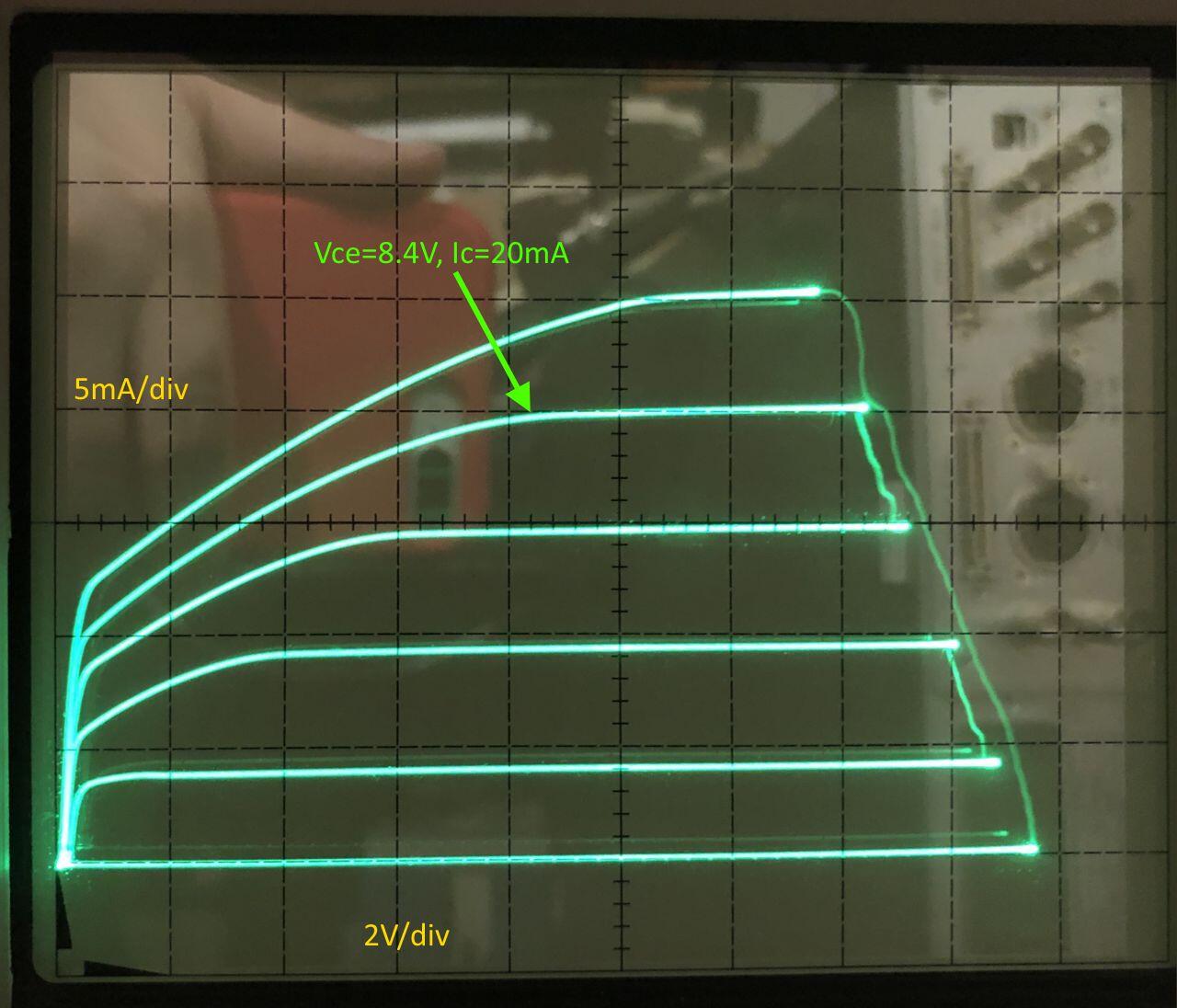
In a previous post I mentioned the less-than-ideal performance when Carbon is powered by a ±400V supply, and I suspected that the lower Vce on the PZTA42 is the culprit. Now it's been proven. The PZTA42 being a high voltage transistor, has a non-linear region at low Vce, as the slanted curves you can see on the upper left side. With 407V on the negative rail, the transistors on my board works at Vce=8.4V and Ic=20mA, right around the knee. The global negative feedback would have a hard time correcting that non-linearity. It also explains why some people prefer setting the Carbon at a lower current when powered with ±400V supply, as it also improves the linearity of the PZTA42, albeit to a lesser degree. I guess Kevin chose the high voltage PZTA42 to deal with the power-on transients. I have a quick and dirty fix. Just bias the SiC MOSFET a little higher to give the PZTA42 more headroom. The SiC MOSFETs are biased by two 175k and an 20k at the gate. Reducing either 175k or increasing the 20k would do. The goal is to move the PZTA42 operating point to the right, well into the constant-current region (parallel lines). I would use Vce=14 to 15V. Pushing it even higher would increase the power dissipation on the PZTA42, eat into the max output voltage swing and have diminishing return. What I did was to put a 260k resistor in parallel with one of the 175k resistors. YMMV because it has to do with the operating point of the PZTA42 in your circuit, the Vgs(th) of your SiC MOSFET, etc. After the quick fix, one of the channels now measures as good as with the ±450V supply. We can see that the max output voltage is slightly less compared to with ±450V supply. The difference is subtle with the log scale, though. Now I'm continue to work on the other channel and see if I can find something else.
-
I only changed the LT1021 with the cheaper LT1236-10. The latter has the same performance as the LT1021 except the long-term stability which we don't need. Oh, and I used the DN2540 in TO-92 package for lower cost. Nothing is different from the original circuit electrically. If the output of the GRHV is low, chances are the passing element (SiC MOSFET) is not damaged. A series linear regulator such as the GRHV is probably the easiest circuit to troubleshoot. Jut need some electronics basics and a lot of patience...
-
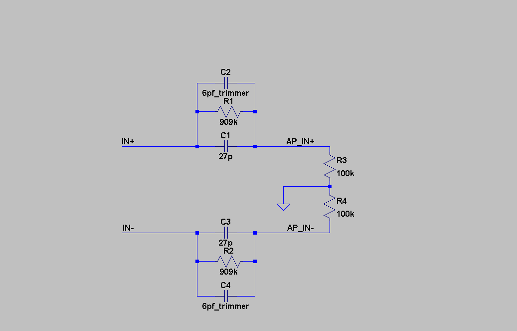
Here is the attenuator I used (R3 and R4 are the AP input resistance, and not part of the attenuator). The R and C are rated at 500V or higher. The trimmers are adjusted with AP analog loop-back (repeat the below till both are satisfied) 1) Amplitude vs frequency response as flat as possible up to 100kHz balanced (I was able to reach ±0.02dB). 2) Set the AP output to balanced-grounded, short the AP +/- input to GND, one side at a time. Adjust the trimmers such that the response of the two attenuator arms are the same. I could use the common mode test feature on the AP to do this, but I figured the amount of work would probably be the same.
-
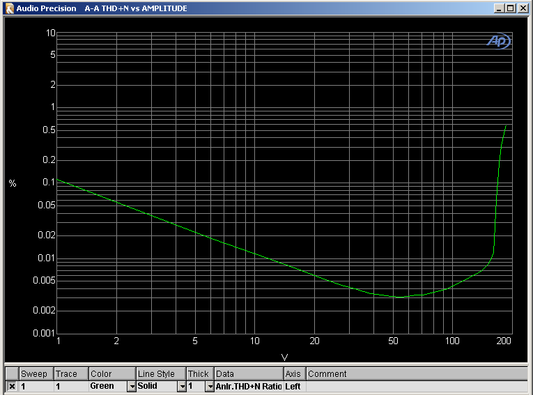
I'm glad to report that both the GeneSiC G2R1000MT17D and the Microsemi MSC750SMA170B work well on the KGSSHV Carbon. The G2R1000MT17D works on the GRHV, too. The overall performance of the Carbon is stellar. It's virtually distortion-free to about 200Vrms at the output, and maintains very low distortion up till 600V!! You want the ±450V power supply for the Carbon. With ±400V I ended up with something like the following. Still not bad but not as brilliant as the curve above. I figured the PZTA42s are not quite in their linear region because of the reduced Vce. A word of caution is that both SiC MOSFETs are somewhat 'fragile' compared to the Cree/Wolfspeed C2M1000170D, especially the G2R1000MT17D. I killed a few when matching them on my curve tracer. I guess the Left-right switch on my curve tracer doesn't guarantee that S connects first, then G and then D. No more failures after I connected a 10V zener diode between G-S on the test fixture. An expensive lesson learned😅
-
Share your favorite stores and parts here.
simmconn replied to omendelovitz's topic in Do It Yourself
Just missed a Yahoo Japan auction on Buyee with tens of J74s, K170s, K117s and more, for just 1Yen starting bid (yes, 1 cent USD). I haven’t figured out how to make Buyee reminders sent in regular hours in my time zone. By default the emails arrive when I’m asleep (Pacific time). btw, I found some C3381s in a local store, BL and GR grades, looks authentic. Maybe I can open a group buy sometime.
.jpg.fca243a99209d9c8c6bdecd89e75ec35.jpg)
.jpg.9ada6f9ba1eda2e31beb9f991e20a5d3.jpg)
.jpg.b649e41bed93ad5ac54e67f6c9030b9c.jpg)
.jpg.5635ea293fec791e3c00289859e74d05.jpg)