Jump to content

luvdunhill

High Rollers
  • Posts

    13,697
  • Joined

  • Last visited

  • Days Won

    38

Everything posted by luvdunhill

  1. geez, are we going the have the "my Xmax is bigger than yours" worm-hole discussion? edit: heh, posted at the same time as Tkam
  2. Please dispose of those two, large round canisters properly by sending them to me. Thanks!
  3. one thing to do at a minimum is work a way to add a test point in somewhere, so we can easily measure across the output resistors to set the bias. This has PPAv2 type slip ups written all over it. I started installing the transistors, but thought better of it after 6 or so. I want to verify the schematic to make sure I get the polarities right.
  4. one other option.. you could easily make the two paralleled transistors before the buffer face each other (flat side would mate on the silk), as well as the two transistors in the CCS so that their faces could be bound together with a zip tie and some thermal grease. (so, all the non buffer transistors could be bound together in pairs, three pairs total) I've done this and it works very well. You can move a single trace to the top and do this quite easily. I think I'd slightly prefer this. What do you think? Then you'd need a way to mark the polarity, maybe a dot or shaded version of the outline? What other TO-92 silk patterns does EAGLE have? Look at the photo. See how the second row output resistors are almost right up against the Dale resistors? The PRP are a bit fatter in the worse case (their body seems to have a looser tolerance) I think as well. Just a bit more room here would be nice, if you cannot also separate the two output resistor rows. It's really tight in there... what about a hair more pitch, say 0.5mm? This is probably more important, as the PRP resistors are kinda fragile if you slam the leads against the body like we need to here. The larger pads seem very doable, as I'm looking at the silk now and would be greatly appreciated. perfect! I think we can safely remove C32B. The other input capacitor is basically equivalent, and this way is better given the feedback capacitor. The mica option for the feedback cap doesn't quite fit. I dunno why CDE has odd pitches, but I'd look at the datasheet for the one in the BOM and make the distance from the second hole from the bottom to the top hole this exact pitch, as I had to really shove it in to get a good fit... If you look at my pics, I'd move in the 2SA1139/2SC3381 pairs towards the middle of the board about 1mm or so (I'll measure to be exact, but look at the one on the right in the pic, you'll see how much room you have). The fins of the heat sinks are very close to the resistor leads. We will almost assuredly have to move the two JFET pairs closer. I didn't have time to build and document how to put these together tonite, so perhaps tomorrow I'll get to it. edit: so you see why the silk is confusing for the regulators by looking at the pics.. alternatively / in addition, we could put surface mount parts on the bottom of the board, but I think just using the TO-92 parts and scrapping the TO-220 silk is fine... Anyways, things are looking like I'll power it up on Friday late or Saturday evening.
  5. Sorry, the Audio-gd Phoenix design looks like shit.
  6. A few pics that illustrate some of my points above:
  7. Tickets from Austin to San Francisco and Vegas to Austin for the whole family! Now to attend to other planning details I suppose.
  8. eh, you lost me after the drill part
  9. I'll check tonite, but these should fit fine for the 7zip packages. Would that suffice? Mouser 575-410322010
  10. well, I have the boards and have started working with one and getting the other ready to send to Kevin. Not an easy board to stuff so far... A few initial suggestions, in random order: 1.) The silk is sort of messed up in places. Kinda like printing on a bad ribbon, for those that remember those days, it's offset at points. I'm assuming this is an issue with the fab, not the files? 2.) The output transistors I think could be better labeled using "2SJ" and "2SK" rather than Q27-Q34. I'd remove that A17,5mm text as well (whatever that means). 3.) The top ground plan extends too far and will be under my aluminum angle, which I'm uncomfortable about. I'm not sure if this will be the case for everyone, but I'd like to move back the ground plane to the most northern edge of the pads. This will cause some of the ground plane in the middle of the output devices to be unconnected and thus removed, but this is okay. 4.) The "1145 / 2705" legend will be partially hidden by the bracket. I'd move it down a bit. Also, perhaps another legend would be more appropriate, as there are four transistors in the middle that are at a 90 degree angle and have no reference designators that I need to track down on the board files to see what polarity they are... maybe add a dot to all the 2SA devices right above the center pin? That way you could accommodate the mystery devices in the middle of the board that are currently at a 90 degree angle from your legend. 5.) If at all possible, there needs to be more room around the output resistors. Especially between R53,R54,R49,R50 and the row below it (R44,R46,..). The bodies on these three rows of resistors practically touch. Any more room would be greatly appreciated. Looking at the layout, you can create some more room at the bottom quite easily. Move the JFETs toward the power connector and move the regulators around a bit and move up R57,R58, etc. You get the idea. More room between the first row and second row of the output resistors, as well as more room between the second row of the output resistors and the R44,R46... row. I think we definitely need to do this. 6.) R33 and R32 actually touch the caps. These should be moved out a bit, you have plenty of room. 7.) On most the caps, I'd remove the "A" and "B" nomenclatures. It gets confusing. Less text is better. Also, I'd remove the smaller silk screen and just keep the larger outline on C11B, C12B, C13A, (and the unnamed capacitor to the right of the power connector), C32B, etc. It's clear enough with the single large outline with the four pads inside and helps the silk look less busy. 8.) The resistor between R28 and R32 has no printed reference designator, that I could find. 9.) On C1B, the south hole could be enlarged a tiny bit, as I cannot quite fit my capacitor in there. I can give the component dimensions, but my guess is as large as the IN connector holes would be great. While everything fits, it is tight in there. I'd move C11B to the left a bit and then C1B to the left as well, since currently everything touches. *10.) In my opinion, the resistor foot print is just too small. I know it will be hard to enlarge it, but I think a lot of people aren't going to like the fact that you have to slam the leads against the body and then the ring gauge on the board is so darn small. I realize it's work to fix this, but I think it will be worth it, as it's very, very tight. I'm just preempting Pars complain on this matter I dunno what to say... it's very, very tight. 11.) I'd add a silk layer to the bottom to explain the rather clever jumpering system and a note to the top of the board explaining that the bottom jumper must be populated. I didn't even notice it myself until I looked at the EAGLE files. 12.) For the four 7zip patterns, I think this will be confusing to stuff, since we're using the small device heat sinks. I know mistakes will be made and people will have to consult the data sheets as is. See attached image for what I'd recommend to do here for the silk. 13.) Depending on the connector you want to use for the 4 pin SIP to the left of the power connector, I'd recommend putting a bit more space between here and the cap. For example, you might want to use a Molex KK connector that has the retention clip, and currently it wouldn't fit. 14.) For the two regulators, I'd use the TO-92 silk pattern. Since the higher voltage parts aren't available in TO-220, I think we should just use this pattern and emphasize this on the silk. The polarity needs to be marked somehow as well. Ok, more tonite after I finish stuffing the boards. Simply a gorgeous design, by the way... hats off!
  11. I think I heard that phrase last time I was in London, and it wasn't a good thing...
  12. I'd love to give this a go.
  13. yup, balanced outputs.. and more gain then you'll ever need Also, in this same class, the Klyne Model 7PX3.5/B has balanced outputs.
  14. I think the manual for the Ayre P-5xe shows how they recommend to build the XLR to RCA connectors, if I'm understanding what you plan correctly. If not, then please ignore.
  15. If this is the case, make those XLR cables as long as you'd like. Especially if you are using solid state stuff. What about the Aqvox? It's pretty decent sounding, IMHO. Also, the Ayre P-5xe, depending on the price these days.
  16. As close as possible, not only for noise reasons, but the longer cable will effect the frequency response (ahem). it's quite easy to calculate if you know all the variables. I'd need to know: inductance of the cartridge (sometimes given by the manufacturer) coil resistance of cartridge (again, given by manufacturer) resistance of cable (per foot, or for 0.5m and 7' say) capacitance of cable input resistance of phono stage input capacitance of phono stage It might be hard to gather this data, but if so, you can easily model the difference and even calculate an optimal loading with the longer cable. I could help you, or you could read and use the calculators here: http://www.hagtech.com/loading.html
  17. 17 foot cable is just asking for trouble on many fronts. It would be much better to run the amplified signal that distance, or consider a wall mount shelf at the front of your system.
  18. I'd love to join a forum about (looks around for nate) fora.
  19. that could be exciting
  20. He might try and sell one of my kids while I'm there, who knows Thanks for volunteering someone else though, I really appreciate the thought and effort
  21. The TO-220 on the left is a regulator, you can see from the side shot. From the top shot you can see they are all National devices, hence my deduction. The soic devices are probably relay drivers, that would be my guess at least. It could be a double sided PCB I suppose.
  22. Hey, probably not the best place for this, but what the heck. I'm lazy. Anyone know of good accommodations (cheap, free, etc.) in the SF area for a family of four? Some sort of kitchenette would be nice
  23. The question I have is are all those TO-220 devices regulators? Sure looks like it. That means this is basically a chip amp...
  24. This graph is worthless without the compliment devices, but ...
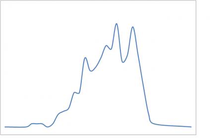
  25. excellent! So, on that note, despite the fact I'm not finished with the n-ch MOSFETs, I feel that I will in fact have a few matched devices left over from my contribution to the MOSFET order after I take the devices out for another project. After a lot of thinking, I will only be offering them as matched pairs, not quads per the rest of the group buy. Also, I'd like to sell the rest of the devices with them, excluding the JFETs (unless they don't sell and I get really, really bored). I'll make sure to order enough boards to cover these possible builds as well. I'm tempted to ask the same price as the group buy ($60 a board), despite the reduction in parts, just due to the unforeseen additional effort with the MOSFETs, and the fact that it's pretty hard to get decently matched pairs without buying two times the needed devices, so I feel that the market will bare this price. I plan on posting a graph for the p-ch parts sometime today and you'll see what I mean I want people to realize that these aren't just sub-par matches, but in fact are even better complimentary matches than the other sets, just not available in quads, which really makes this possible as they are drawn from the "tail" of the distribution. Please PM me if interested.
×
×
  • Create New...

Important Information

By using this site, you agree to our Terms of Use.