

Leaderboard
-
MexicanDragon
High Rollers12Points8367Posts -
Grahame
High Rollers6Points16729Posts -
mikeymad
High Rollers6Points13720Posts -
Hopstretch
High Rollers5Points16781Posts

Popular Content
Showing content with the highest reputation on 07/15/25 in Posts
-
LOVE this group, and they're finally back together after a decade and change break. They dropped a brilliant Tiny Desk Concert; I may need to watch it again.3 points
-
You don't need another Camera, right @blessingx?2 points
-
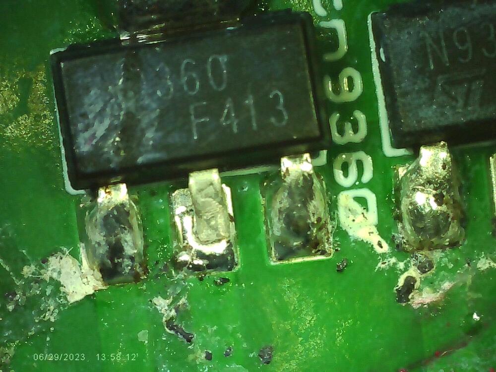
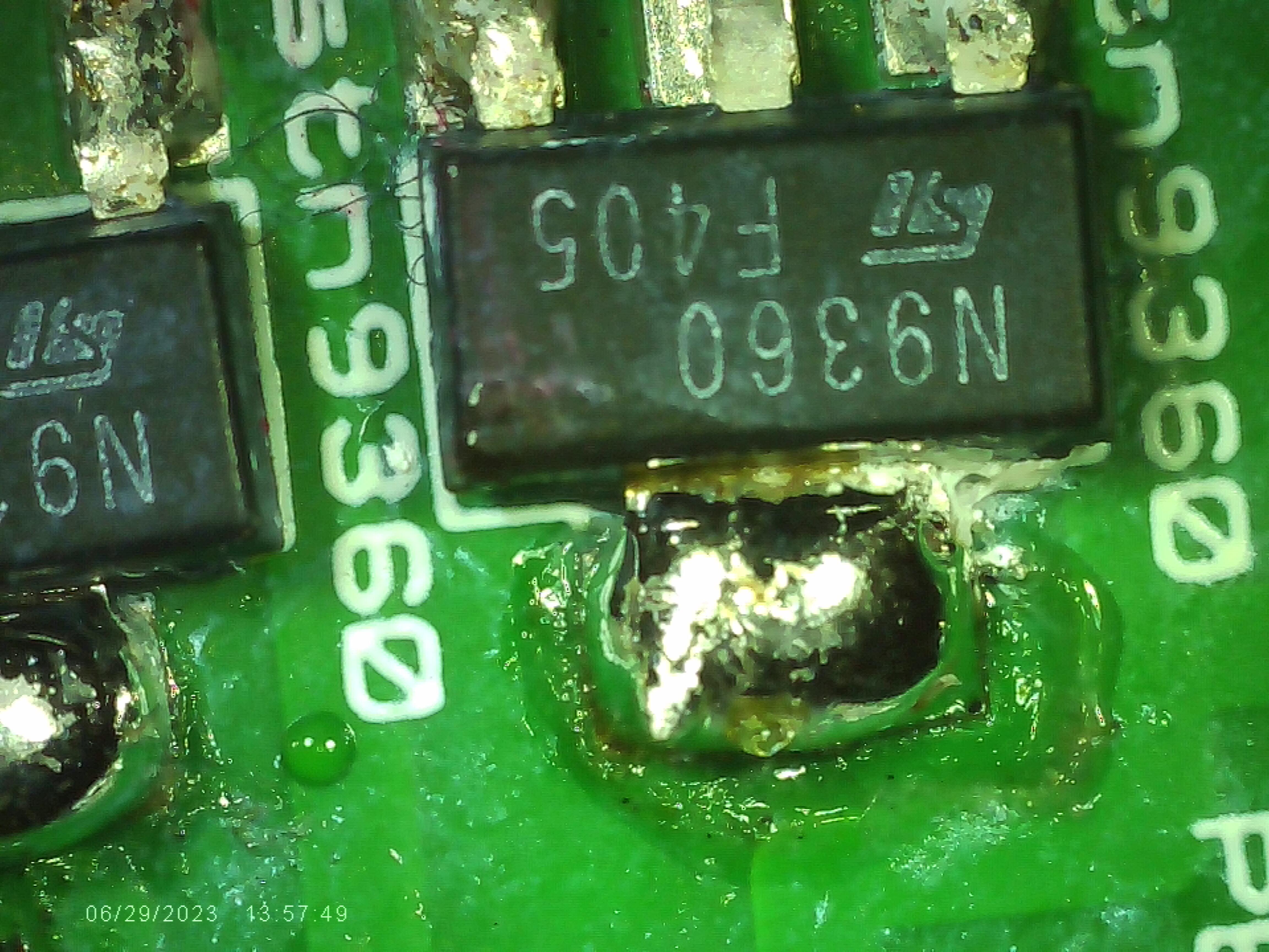
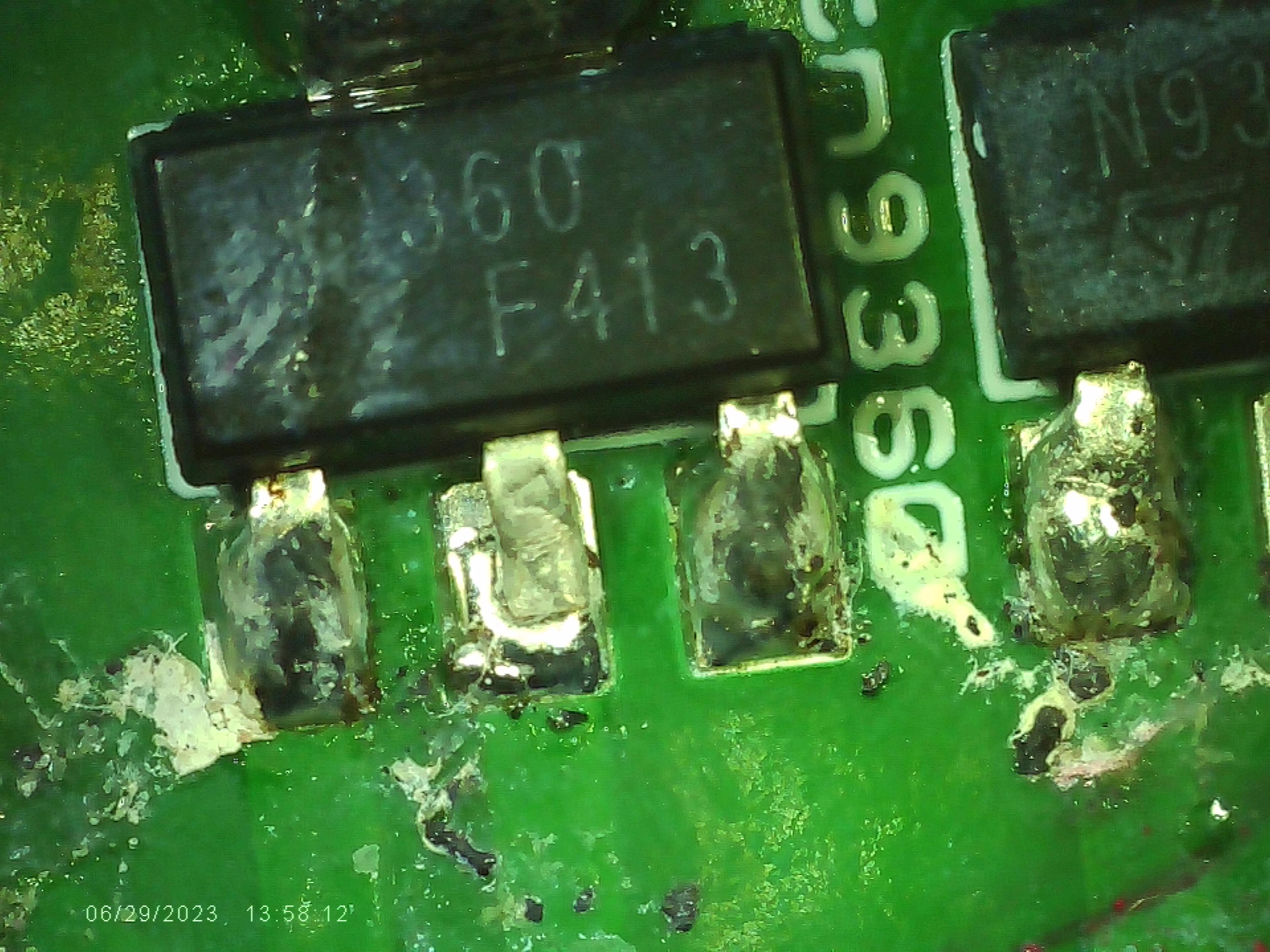
2 points1 point1 pointIf you use them in a constant current source, the Vbe-Ic curve (figure 10) is probably more important than hFE. If you don’t have ways to measure, pick two that are closest in hFE for each channel and hopefully they come close in other parameters as well. If you ask me, I always order at least 2x more than the BOM qty and match them on a curve tracer at or near the actual operating point. The bigger the pool, the more likely you’ll end up with well matched pairs.1 pointSix Degrees of Inner Turbulence by Dream Theater (2002) https://album.link/frb2khtqzt3f9 Example: Realizing there were a few gaps in my Dream Theater history. Filling those gaps. Happily.1 point1 pointNote, not my soldering job. battery in microscope dead too much work to get the 1:1 lens out.

 1 pointLots of Luedji Luna. Lots and lots. And just a little extra.1 pointUnusual Weather by Michael Manring (1985) https://album.link/kcfjzcvstwqth Example: It has been too long since I have listened to Michael's fretless bass. I have this on vinyl, but that is in storage, which is sad. But music is still good.1 point1 pointStax just posted this on X in Japanese but it made me laugh: Anybody want to venture a guess why this had to be posted? Terrible headband design strikes yet again.
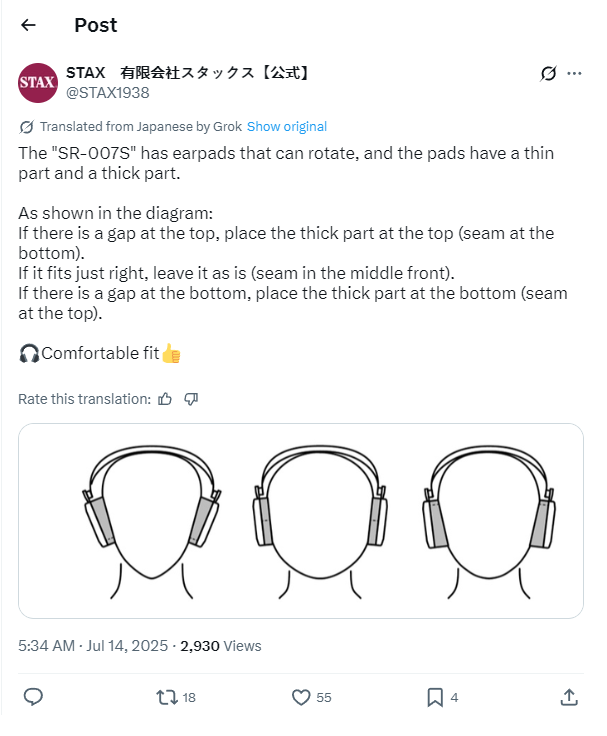 1 point1 pointThe slatted door style has a lot of intricacies and places for failure. It looks simpler than the actual design. Many dados and places where parts have to fit exactly. But they went together easier than either of us expected. Not an accident, but Al's planning and forthought. Absolutely worth the effort, as they'll be an eye catcher for sure. This has been a rewarding project in several ways. Now that I'm no longer working as a carpenter, it's my much needed release for creativity. And Al and I are really enjoying the woodworking and smashburgers.1 point1 pointAre you having a good time, Belvedere? Hip Service were. Serving up a diverse collection of crowd pleasers. Jackson 5, Beyonce, ABBA, Journey. Tight.

 1 pointJust in case someone can make use of this one way or another. https://www.goodreads.com/book/show/215798863-audiophile
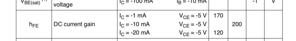
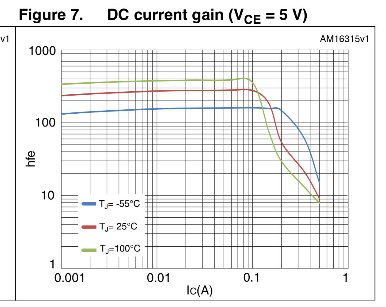
 1 point1 point1 point1 point0 points0 pointsIf I were to choose from a well executed raster image logo in the marking and a badly burned vector one, I’d opt for the latter in a heartbeat. I’ve explained the reason and would not repeat here. For the hFE, you need to know the Ic and Vce your testing was performed at, in order to make a meaningful comparison with the numbers in the datasheet. If you don’t know, measure them. The datasheet says minimum hFE is 170 at 25 degree C, Ic=-1ma and Vce=-5V. From the chart you can see hFE goes slightly up from Ic=-1ma to -10ma and then to -20ma before it starts to drop after Ic=100ma (the red line). If your sample tests at hFE=150 between Ic=-1ma and -10ma, it’s below spec and would be a reject by the factory. You can see the red line is well above 200 and approaching the 300 line, so 340 is not a surprise. +/-20% is considered normal variation. Why would they specify min hFE at only 120 at Ic=-20ma? It could be a simple mistake, or indicating that the hFE could drop as early as Ic=-20ma, unlike what the typical curve suggests, which is a bad news for circuit designers (not applicable for our applications). Nevertheless, sandbagging would not get them into trouble anyways, if you know what I mean. I could go on and on and brag about my affiliation with the semiconductor industry, but let’s keep the personal information out of this discussion. If you think my comments make sense, think about it. Otherwise, just take it with a grain of salt.
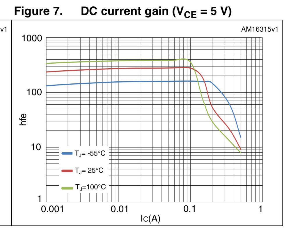
 0 points


Important Information
By using this site, you agree to our Terms of Use.
Account
Navigation
Search
Configure browser push notifications
Chrome (Android)
- Tap the lock icon next to the address bar.
- Tap Permissions → Notifications.
- Adjust your preference.
Chrome (Desktop)
- Click the padlock icon in the address bar.
- Select Site settings.
- Find Notifications and adjust your preference.
Safari (iOS 16.4+)
- Ensure the site is installed via Add to Home Screen.
- Open Settings App → Notifications.
- Find your app name and adjust your preference.
Safari (macOS)
- Go to Safari → Preferences.
- Click the Websites tab.
- Select Notifications in the sidebar.
- Find this website and adjust your preference.
Edge (Android)
- Tap the lock icon next to the address bar.
- Tap Permissions.
- Find Notifications and adjust your preference.
Edge (Desktop)
- Click the padlock icon in the address bar.
- Click Permissions for this site.
- Find Notifications and adjust your preference.
Firefox (Android)
- Go to Settings → Site permissions.
- Tap Notifications.
- Find this site in the list and adjust your preference.
Firefox (Desktop)
- Open Firefox Settings.
- Search for Notifications.
- Find this site in the list and adjust your preference.