
jamesmking
-
Posts
420 -
Joined
-
Last visited
-
Days Won
1
Content Type
Profiles
Forums
Events
Everything posted by jamesmking
-
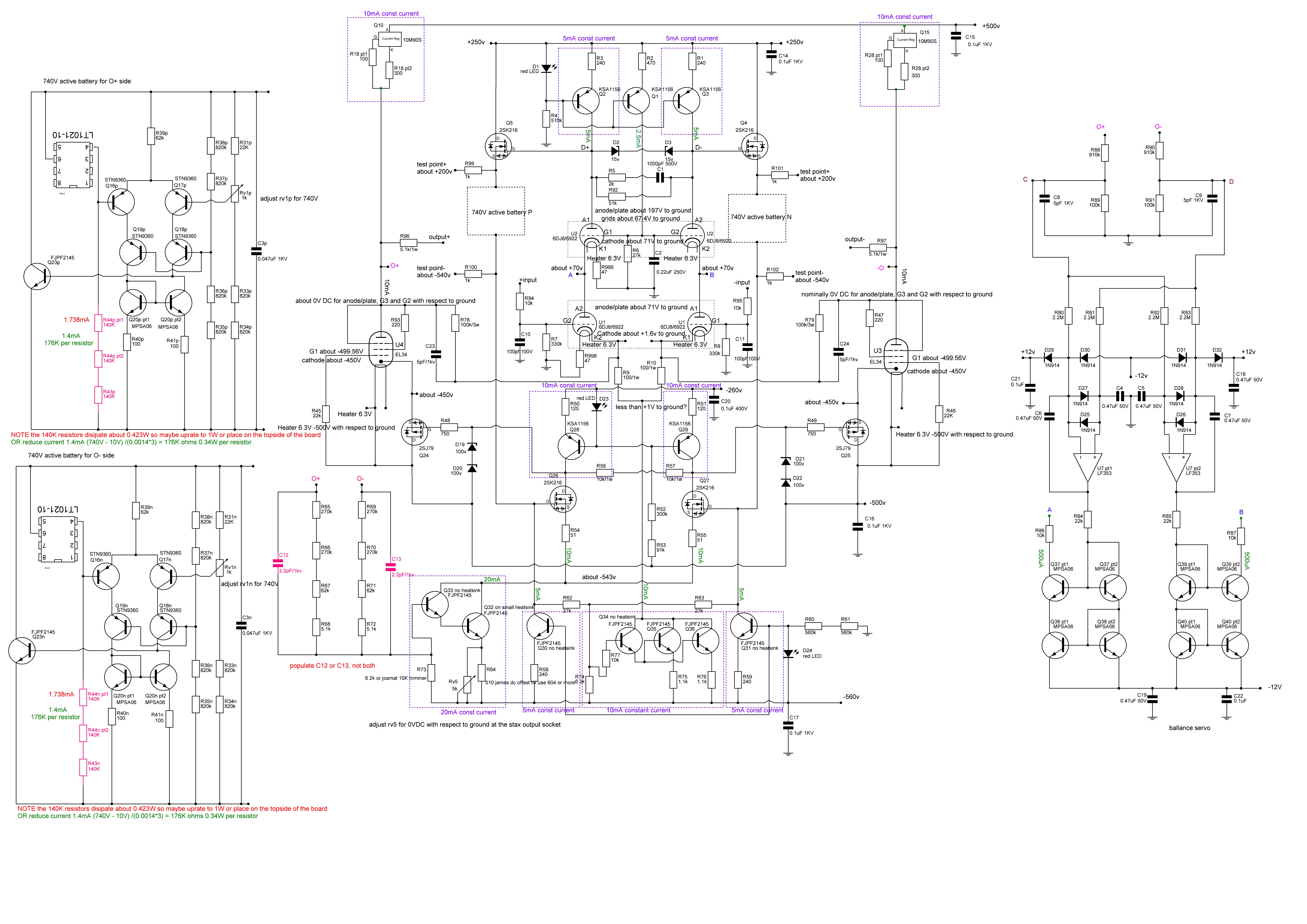
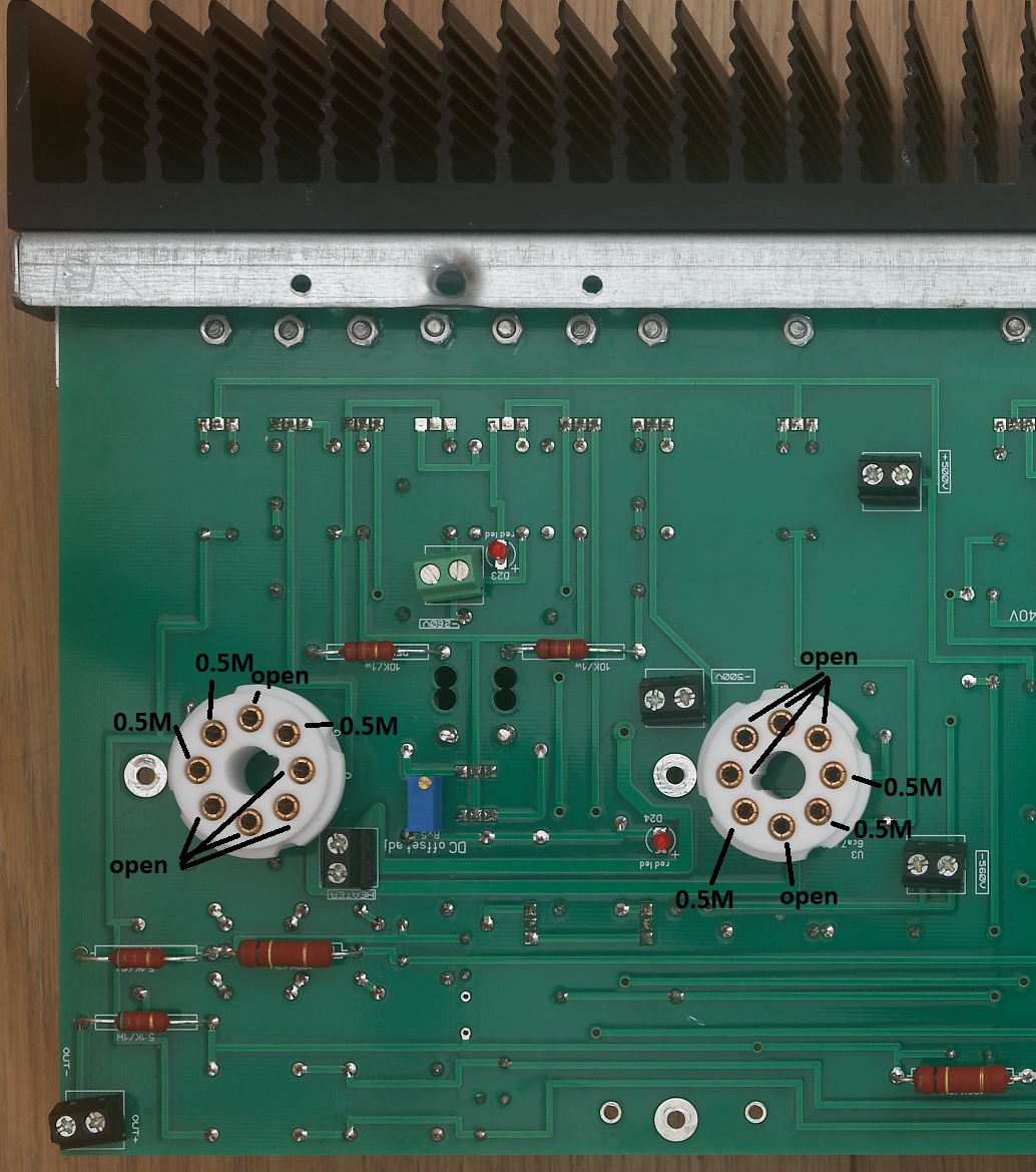
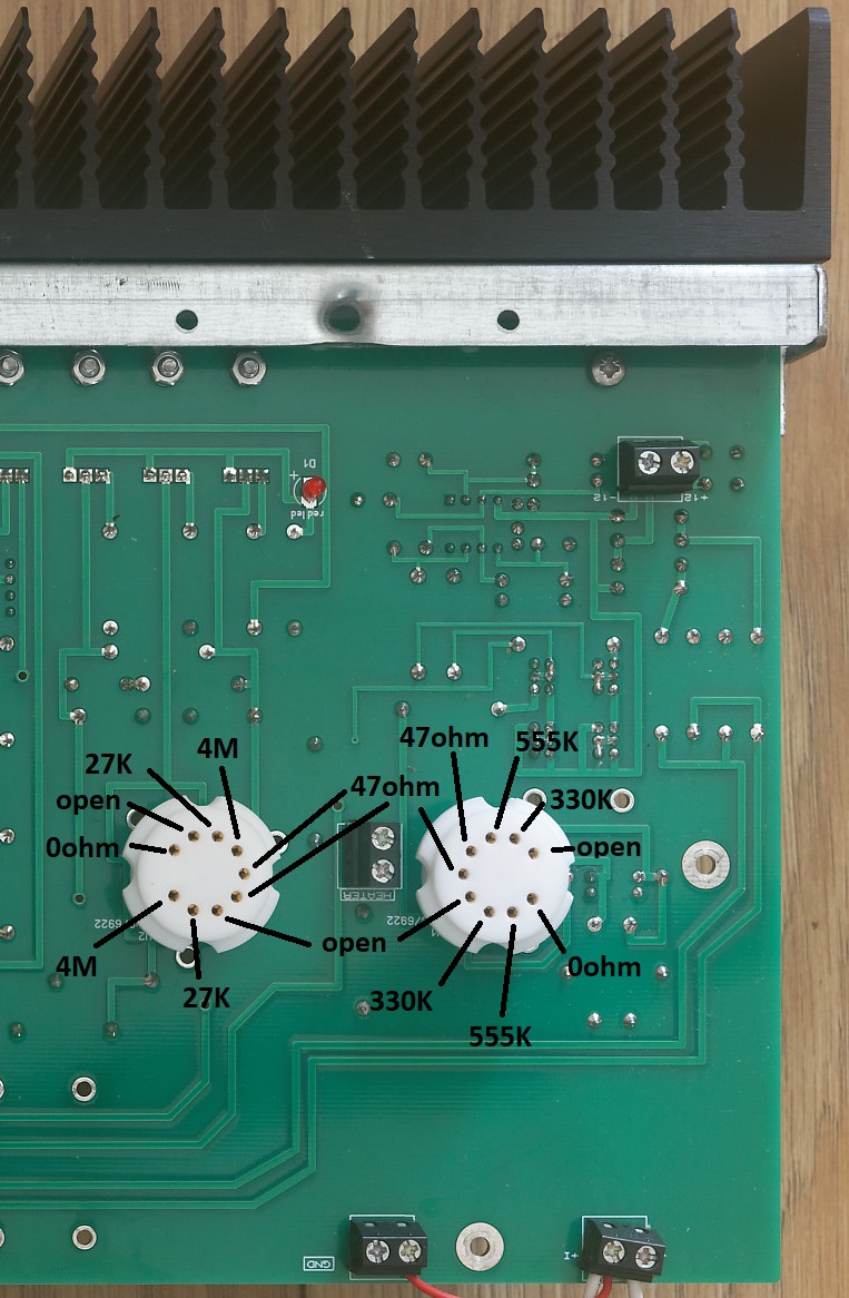
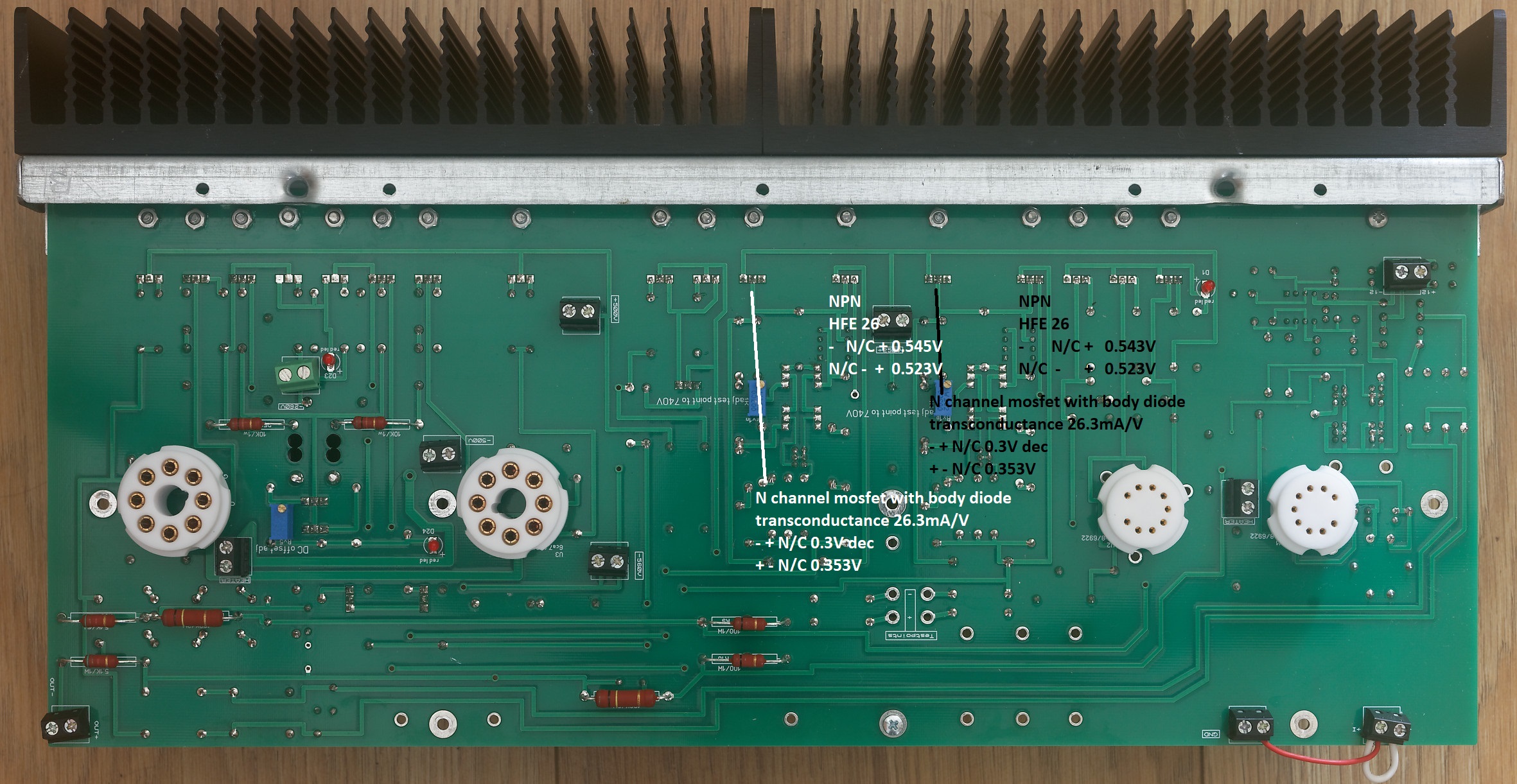
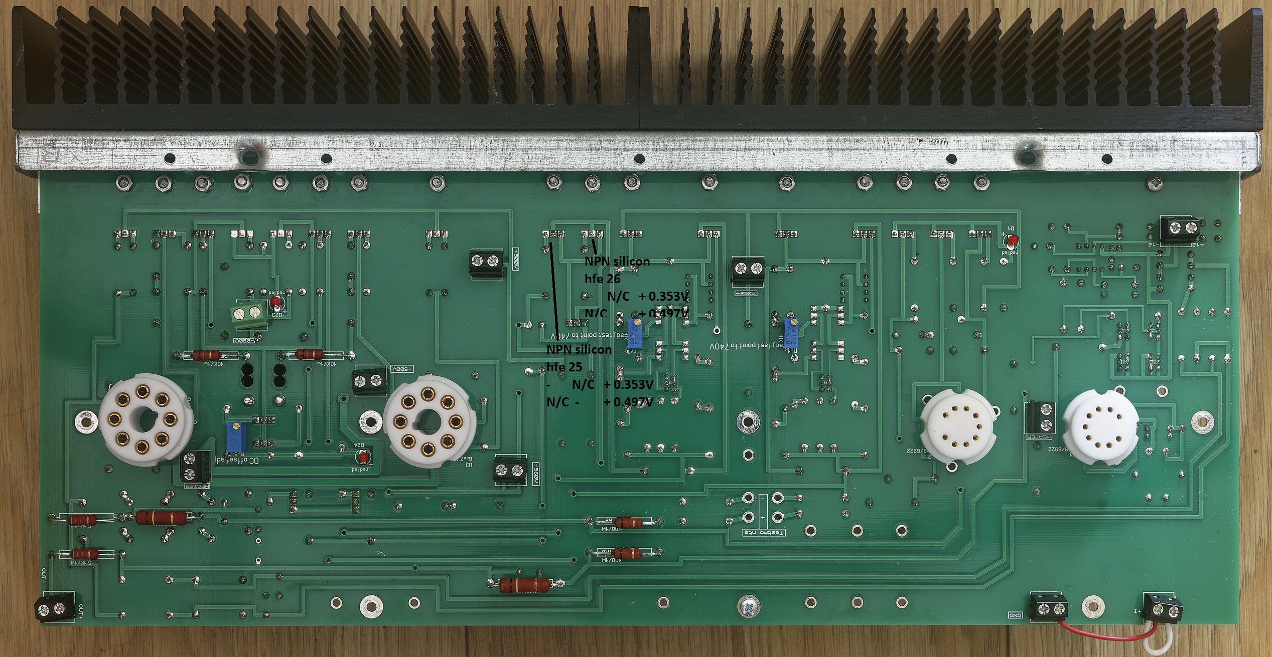
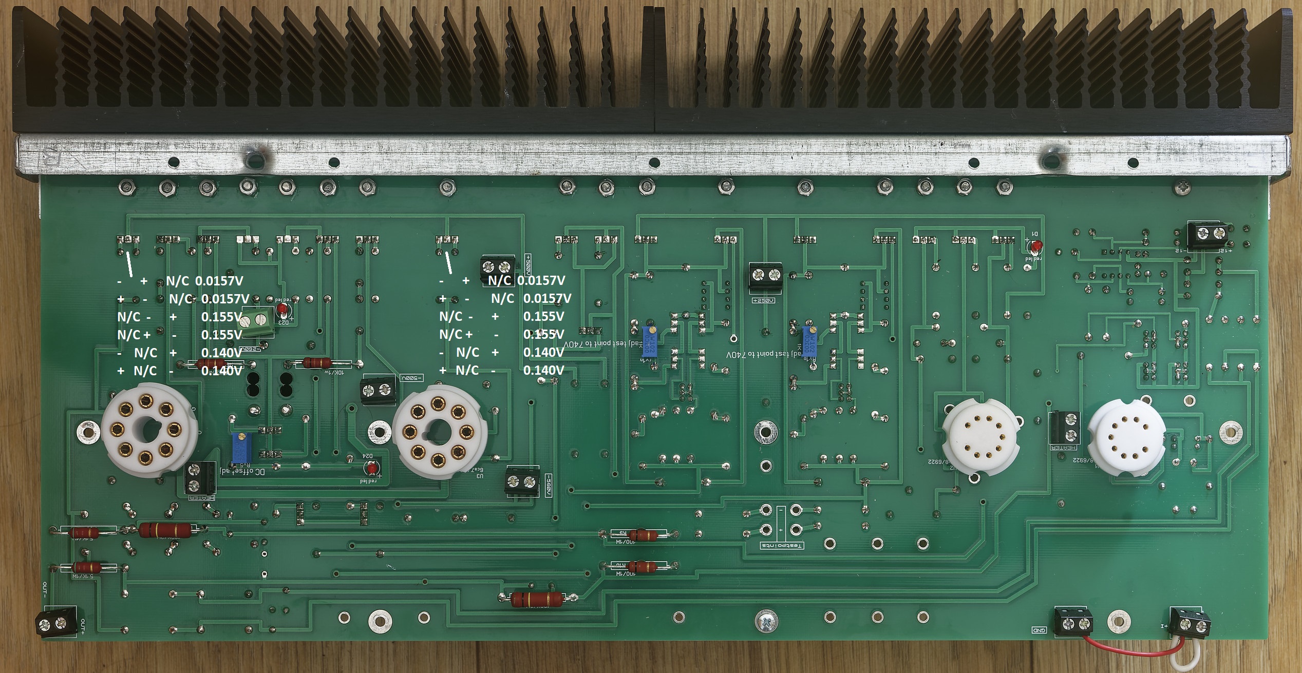
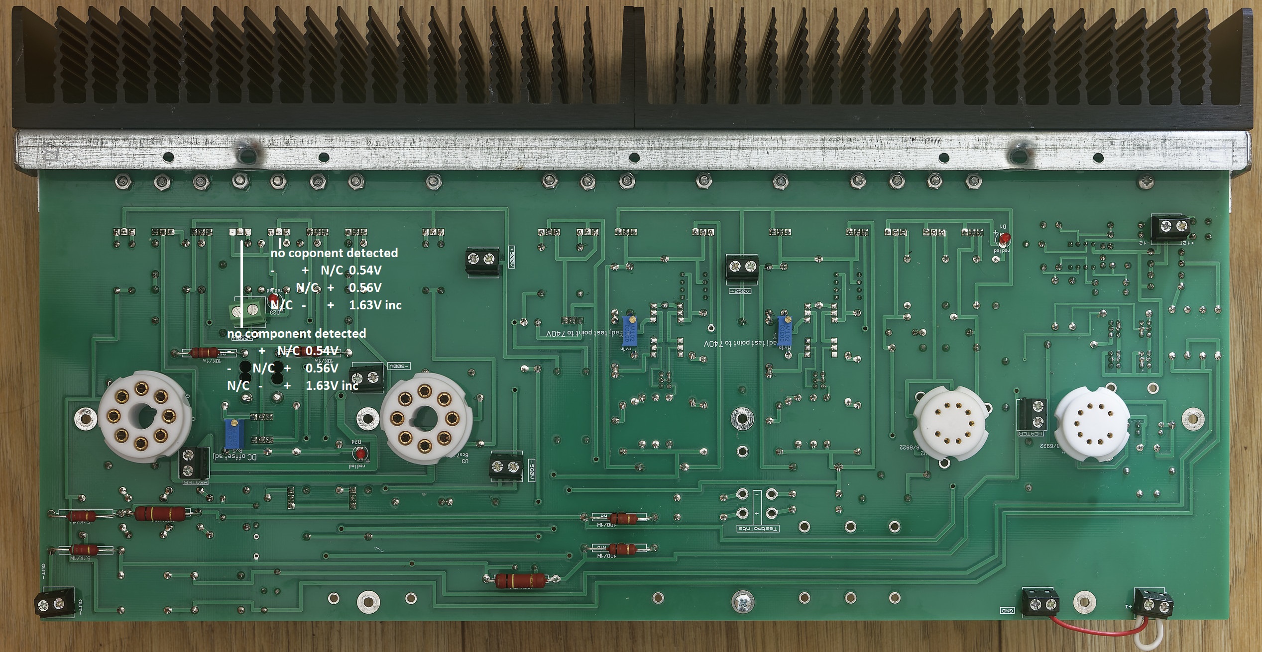
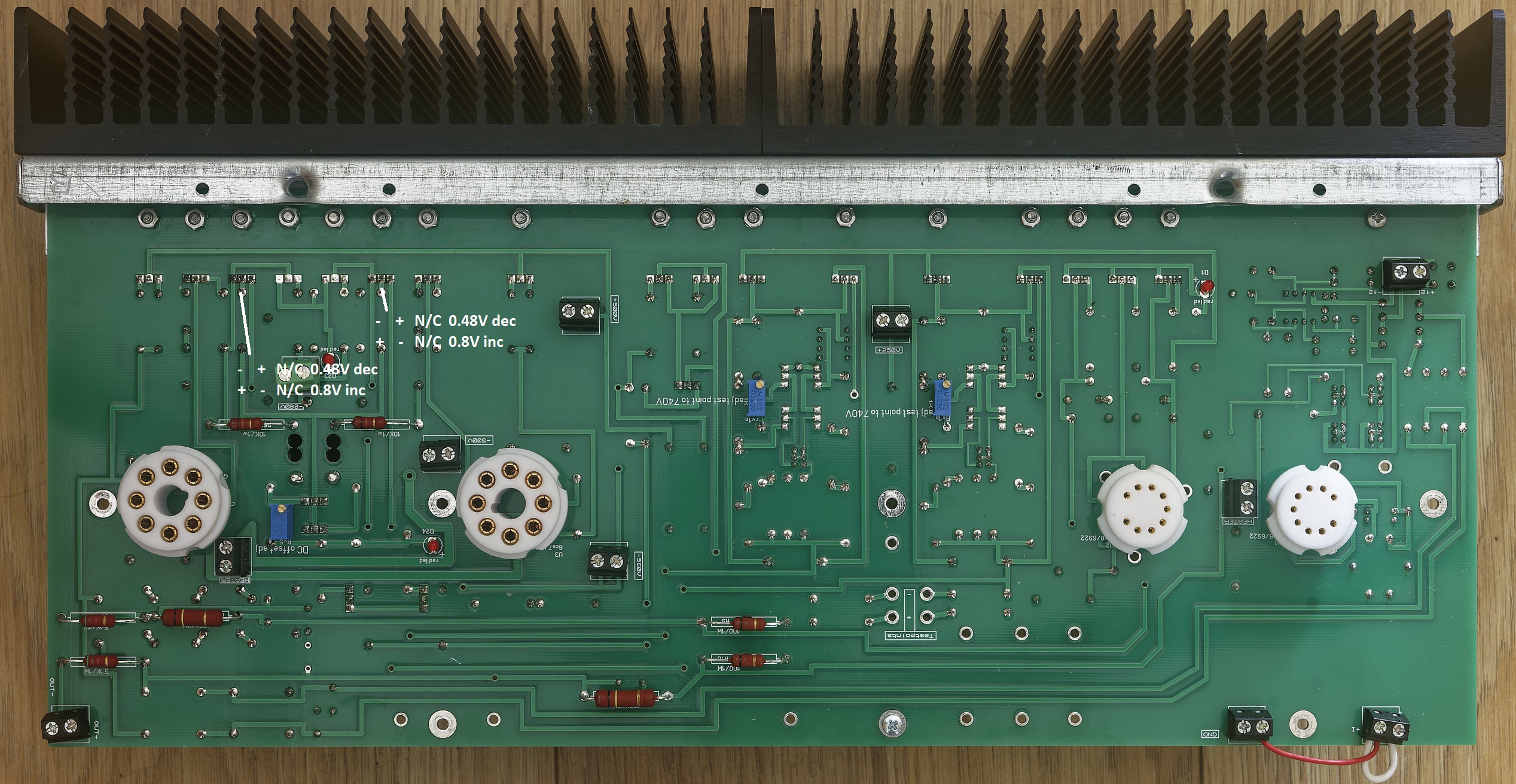
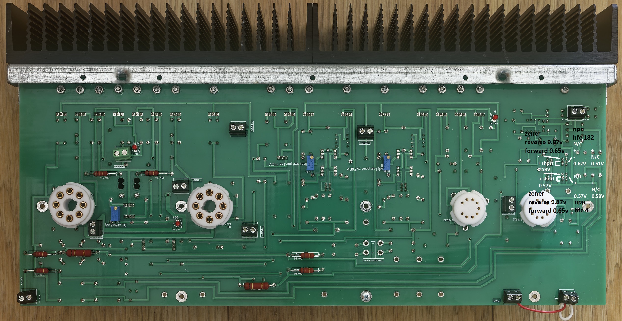
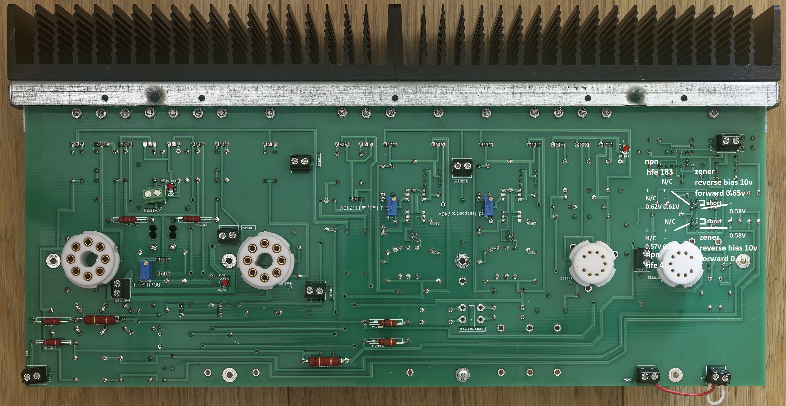
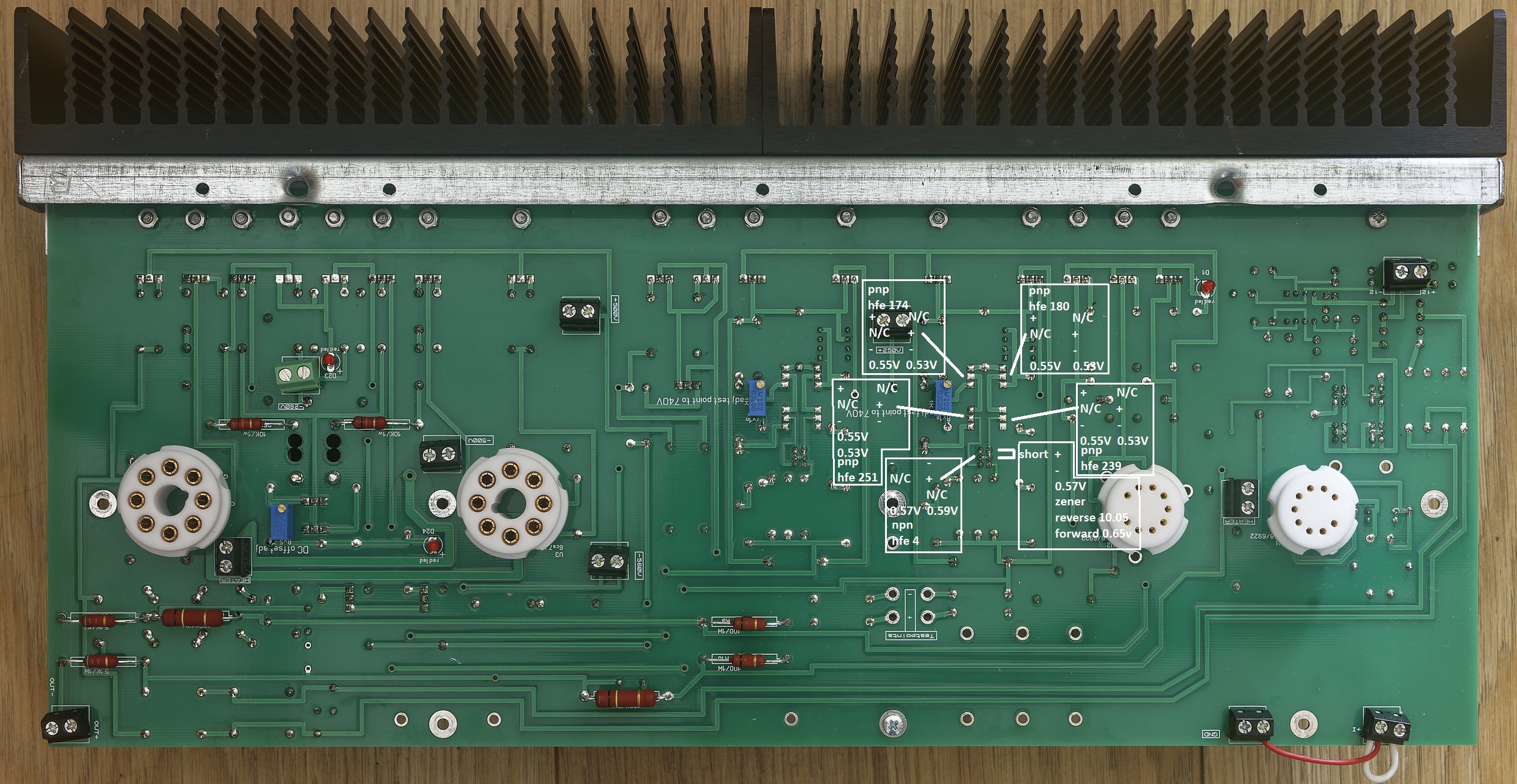
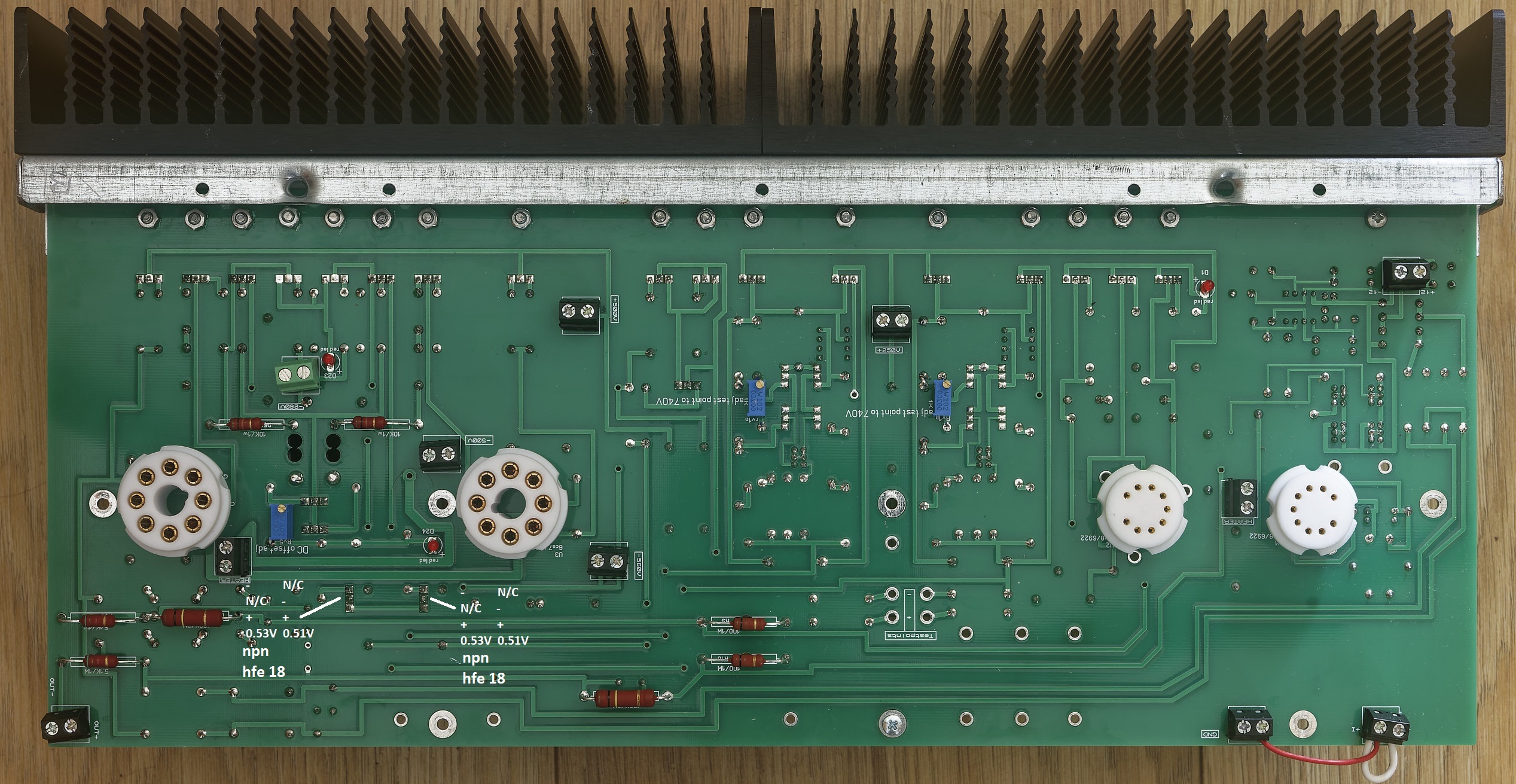
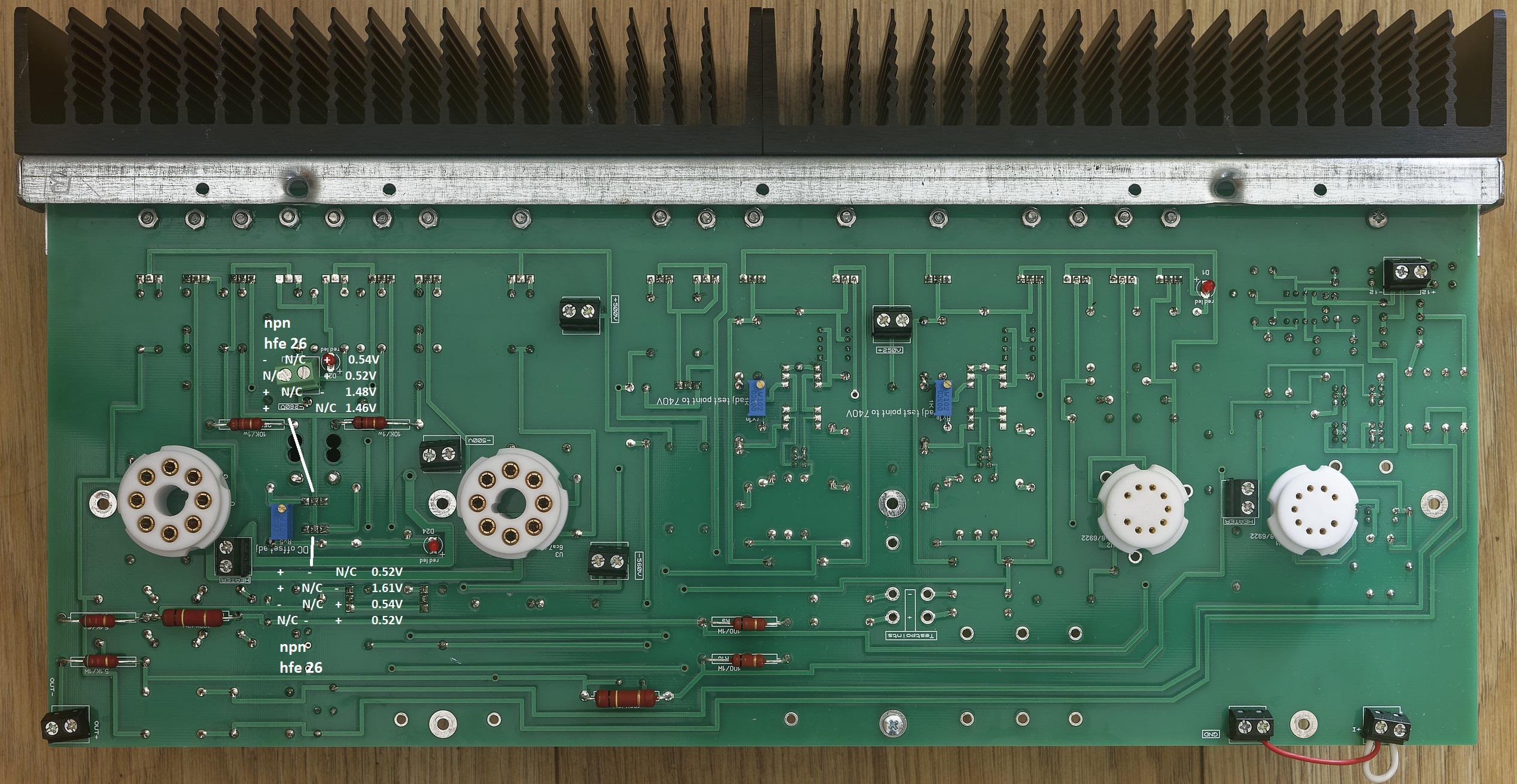
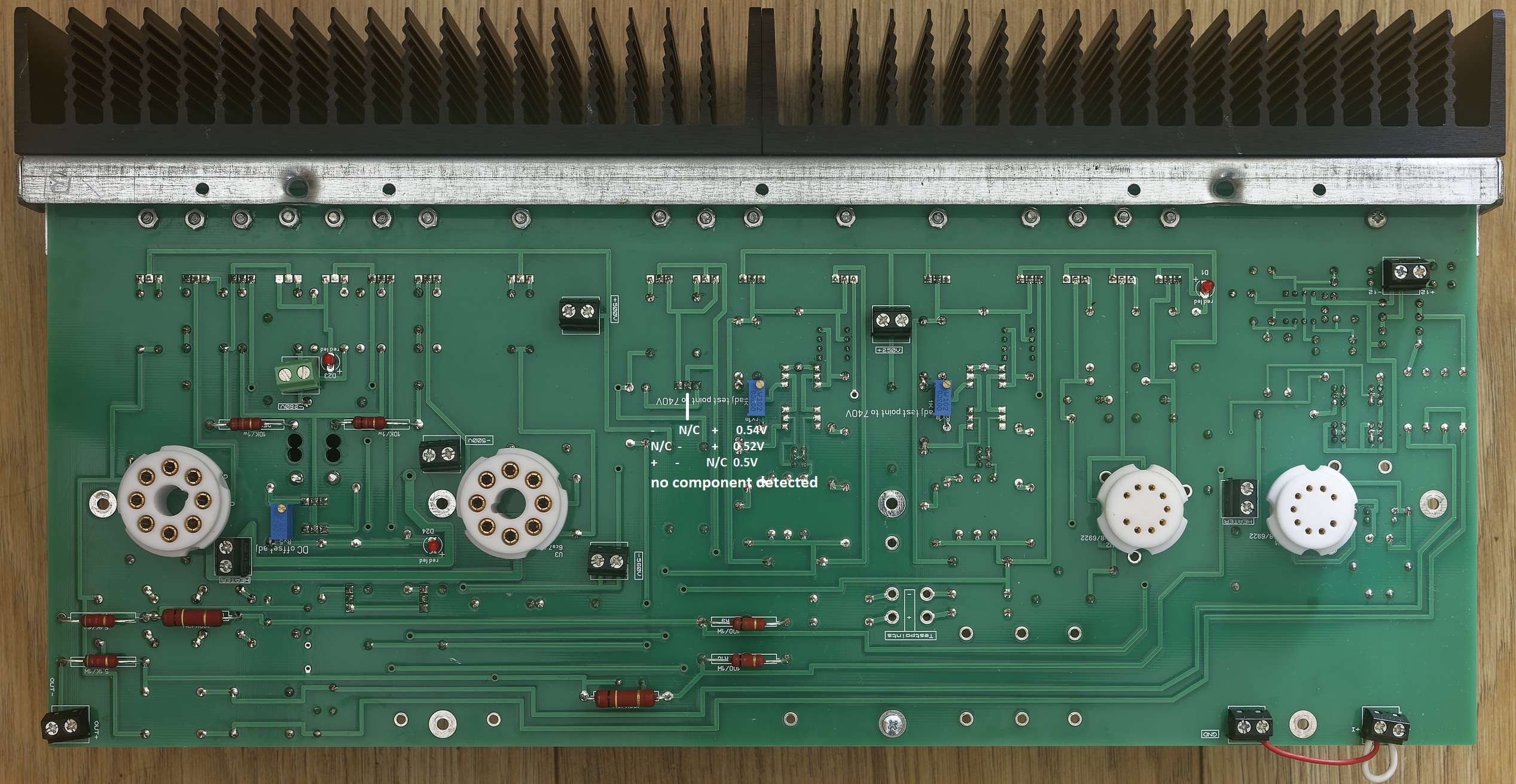
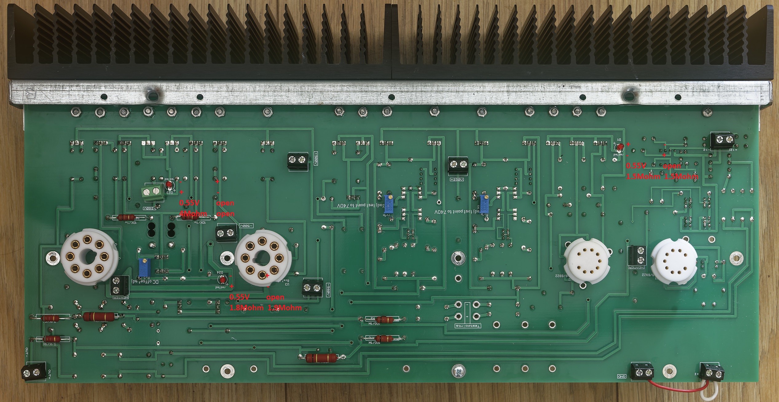
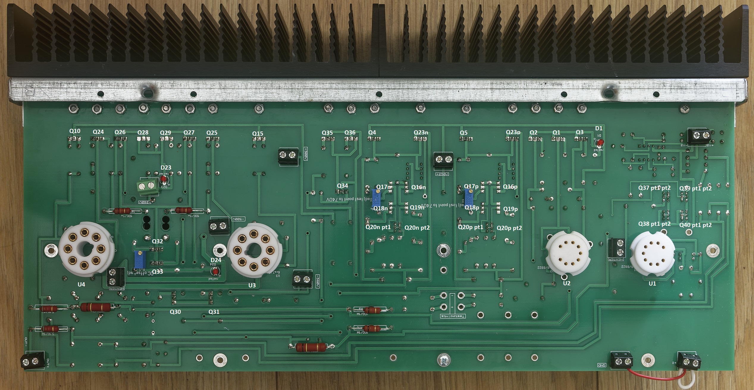
The unofficial mostly modern T2 troubleshooting and verification guide. Weclome, this guide covers the mostly modern T2 which has the following schematic: The gerbers for the amp can be found here: https://drive.google.com/drive/folders/1r3g2TAtBUaBdiMorTWX7yYgeJ7maQbYW and the gerbers are staxt2nc3fdh7.zip The guide is intended for both pre-power on verification of an amp build, verification of voltages on power on and general troubleshooting. All tests are performed using a Brymen BM869s and peak DCA75. Using a different multimeter may effect the results slightly but you should still get similar behaviours and ball-park figures. Transistor and Diode Location Section 1. Build verification with no valves installed and no wires/volume control connected to the amp All of these checks can be performed with a multimeter from the top side of the amp board leds Checks. All 3 leds on each channel should read about 0.55V voltage drop in forward bias (multimeter + terminal/red lead connected to led + and multimeter - terminal black lead connected to led -) and open circuit in reverse bias (swap the probes around) when tested with a multimeter in diode check mode. The leds will not light from the diode test due t the current draw if the components around them. The exact forward voltage drop will depend upon the characteristics of the red led but anything significantly different here indicates a problem. 0 voltage drop in both directions indicates a short across the led or the components it connected to. check for solder bridges and failed short transistors. 0L indicates in both directions means the led has dry solder joints or is blown. using a multimeter in resistance mode check the leds D23 close to the -360VDC psu input. In forward bias expect around 4M ohms. With the probes reversed you should get open circuit. D24 is the led closest to the octal socket for the EL34 and should read about 1.8M in forward bias and about 1.9M in reverse. D1 is between in the 9 pin sockets but close to the heatsinks. This should read about 1.5M in both directions. Readings in both directions of a few hundred K ohms or lower indicate the led may have been leaky or a transistor it is connected to has gone short circuit or a solder bridge. Input terminal checks With the multimeter in resistance mode and the - terminal connected to the amp ground, and the positive terminal connected to the + input of the amp you should get about 340K and the same for the - input. Naturally expect the same results for the other channel. If significantly different suspect incorrect resistors for R94, R7 (positive input). Or R95, R8 on the - input. Output terminal checks With the multimeter in resistance mode and the - terminal connected to the amp ground, and the positive terminal connected to the + output of the amp you should get about 0.5M and the same for the - output. Naturally expect the same results for the other channel. Valve Socket Checks. With the multimeter in resistance mode and the - terminal connected to the amp ground, and the positive terminal expect the following resistances for both EL34s: (socket viewed from the top of the amp). (note the 0.5M reading may start lower and quickly ram up and the small capacitors in the circuit are charged by the multimeter). For the 6922s (socket viewed from the top of the amp) Diode Checks of transistors Note it is possible for a transistor to fail in such a way it has very little gain but still has a diode drop and so diode checking transistors is not a foolproof measure of a transistors health. But 0V drop when not expected indicates a short etc. Diode checks KSA1156 checks Q1, Q2, Q3 two of the ksa1156s (Q2 and A3) measure the same in diode mode the centre one (Q1) differs slightly. All combinations of probes and pins on a transistor result in open circuit unless otherwise shown otherwise: + indicates positive multimeter probe attached, - indicates negative multimeter probe attached n/c indicates no probe attachment. Note: for the other channel EACH KSA1156 is rotated 180 degrees about the y (vertical) axis. Peak DCA in circuit testing Q1-3 The peak DCA 75 identifies all 3 transistors as PNP silicon. The centre with a hfe or around 28 and the other two with slightly higher hfe of 30 to 31. This test is reliable, anything significantly different indicates a problem. Note it is easier to do these tests from the underside although you can hook up the dca proe hooks to something like a sensepeek weighted self standing spring loaded probe tip assembly and test easily from the top (https://sensepeek.com/pcbite-20 Diode check and Peak DCA 75 for Q23P FJPF2145 This is reliably identified as a NPN with hfe 26 and is part of the virtual battery connected to the + output side of the channel. NOTE: It has a mirror image pinout compared to the ksa1156s. Diode check and peak DCA 75 check for Q5 2SK216 This is reliably identified as a N channel mosfet with body diode and has a transconductance of 23.3mA/V. Although not part of the virtual battery it is directly connected to it. WANRING This transistor has a live mounting tab and must be fully insulated from the heatsink. A resistance check from the metal tab to the heatsink it is mounted on absolutely must read open circuit. Diode measurement for this transistor does not show a stable reading. In this case dec indicates a reading that decreases over time. The next two transistors in the heatsink row are Q23N and Q4 which perform exactly the same role and are exactly the same type of transistors as Q23P and Q5 respectively and should measure about the same I got 28mA/V for the Q4 so expect a little variance here). NOTE: on the other channel the order of the 2SK216 and FJPF2145 are reversed. Diode check and peak DCA 75 check for Q35 and Q36 FJPF2145 These are the current providers (driven by Q34) for a 10mA constant current source that feeds the input 6922s. The job is equally divided between them and they should measure the same. The DCA75 reliably identifies them as NPN silicon hfe 25-26 Diode check and peak DCA 75 check for Q15 and Q10 (10M90S) These are identified out of circuit by the dca75 as N channel depletion mosfets. However, in this circuit they provide anode current and are wired in such a way the DCA75 can not identify them and reports no component. The DCA75 should not report any shorts and the metal mounting tab is live and absolutely must be insulated from the heatsink they are mounted on. Q15 and Q10 are identically configured and should measure the same. The gate and cathodes are connected together with resistors totalling only 400ohms so the diode drop voltages will be lower than for the other transistors also unlike the other transistors all combination of probes will result in a voltage drop. The voltage drop should be the same in the forward and reverse directions. Diode check and peak DCA 75 check for Q28 and Q29 (KSA1156) These are identified out of circuit by the dca75 as PNP silicon. However in this circuit they are wired in such a way the DCA75 can not identify them and reports no component. Each should measure the same. Diode check and peak DCA 75 check for Q26 and Q27 (2SK216) These transistors do not produce stable diode voltage drops. Diode check and peak DCA 75 check for Q25 and Q24 (2SJ79) These transistors are not easy to get a stable reading on. Diode and peak dca75 Check Balance servo Q37 - Q40 (MPSA06) 4 of the MPSA06es have their collectors and bases shorted together and so can be considered to only have two pins as far as diode checking concerned. NOTE for any transistor with shorted pins only two dca75 probes were used (one to the shorted pins and the other to the non shorted pin) to avoid the dca just reporting probes shorted. Understandably ni this case the dca75 can not identify the component as a transistor and instead reports a 9.87V zener. All other transistors are correctly identified and hfe provided. Diode and peak dca75 Check Virtual Battery Q16 - Q18 (STN9360) and Q20 (MPSA06) the other virtual battery in the channel (just to the left) should measure similarly and is identically laid out. Q20 pt 1 has collector and base shorted. All 4 stn9360 should diode measure similarly. NOTE for any transistor with shorted pins only two dca75 probes were used (one to the shorted pins and the other to the non shorted pin) to avoid the dca just reporting probes shorted. Understandably ni this case the dca75 can not identify the component as a transistor and instead reports a 10V zener. All other transistors are correctly identified and hfe provided. The stn9360 are pnp and the remaining non shorted mpsa06 as npn Diode and peak dca75 check Q30 and Q31 (FJPF2145) Each transistor provides a separate 5mA current source and are directly connected to the virtual battery. With the led D24 across their base and emitter. Each is identically configured and should read the same. Dca75 reliably identifies both transistors as npn both hfe 18 Diode and peak dca75 check Q32 (on seperate small heatsink) and Q33 (FJPF2145) this forms a 20mA current source which is controlled by Rv5 and sets the DC offset. DCA75 reliably identifies both transistors as npn both with hfe 26 Diode and peak dca75 check Q34 (FJPF2145) Q34 provides control for Q35 and Q36 which creates a 10mA current source. The dca75 says no component detected. <<< IN PROGRESS >>> #include <usual_disclaimer.h> #include <usual_high voltage_warnings.h>

-
update on the RIP T2. The four 270K resistors R65 to R68 are discoloured I believe because of the higher than expected DC voltages across them from the massive DC imbalance. Otherwise there are no visible signs of problems. I found a dead 2SK216 in addition to the dead 2SJ79 on the same channel that the 6922 failed on. Diode testing found the dead J79 but to find the dead K216 I used my peak dca75 to measure the two ksa1156s and found radically different hfe measurements (43 vs 143) so I removed the other J79 and the readings were dd not change. The removed J79 measured ok. So I suspected the K216es and removed them 216es one measured good and one bad. The good K216 was connected to the bad J79 and good J79 connected to the bad K216... The ksa1156es measured the same hfe when the 4 transistors were removed so I believe they are ok. I'm replacing all 4 mosfets with ksa1220A and KSC2690A because that's all I have... The other channel had the same imbalance issues and one of the K216es there is dead too. Both channels now have 1220 and 2690a installed. But I noticed that the ksa1156s on the channel with the failed 6922 measured hfe 51 in circuit and the channel with only the single failed k216 the same ksa1156s measured 2hfe. Hmm... looking at the circuit I decided to measure the resistance across led between the emitter and base of the ksa1156es... channel with the failed 6922 about 150K and about 190K leads revered. Channel with single bad k216 about 3.4M and open when reverse biased... So either the led or the ksa1156s where leaking. Desoldered the ksa1156s and tested them... ok. desoldered the D23 led and replaced it. Now 3.4M and open circuit. So the led had gone leaky. At least both channels now measure the same... The other led close to the EL34 (D24 ) on the channel with the dead 6922 is also leaky . So score so far: right channel 6922 shorted heater to cathode K216 DCA75 measures it as a zener diode J79 DCA75 measures it as two diodes Led Brymen bm869s measures it as a 150K resistor Led Brymen bm869s measures it as a 88K resistor Left channel K216 DCA75 measures it as zener diode
-
I wish you good luck. I can't believe how screwed up Stax as a company is. All they have to do is make the sr007a with spares, support and repair, license the blue hawaii and modern T2 from Kevin and maybe a couple of cheaper energizer designs and they would done.
-
I'm thinking about that. I didn't realise there were so many around. I guess I could cut the legs short and run high voltage silicone wire to the appropriate through holes....
-
In the uk I had a sr007 mk2 cable replacement from electromod (I got the cable caught did not realise stood up and damaged the cable). They may be able to help. Good luck https://www.electromod.co.uk/stax-spares
-
It lives! the son of the mostly modern (RIP) T2 was powered up for the first time this morning (not in a case and with cheap valves) and looks good. All virtual batteries within 0.6V of 740 volts with no adjustments to the trimmers. DC offset after warm up <4V without any adjustments to the trimmers. DC ballance <0.03V power consumption as expected. I did have a bit of a scare. When powering on with my variac for the first time the led next to the EL34 was very dim compared to the others and all the leds where less bright than my original build. Then I remembered that I used different leds in this build and they are in general less bright. I don't think I can be bothered to remove these leds and replace them with the same as the RIP T2. Latest update in the rip T2 troubleshooting, diode testing and comparing the silicon to the son of T2 it looks like one of the J79s is dead... which is a pain since I have no replacements. This dead J79 is on the same channel as the failed 6922. The op-amps and voltage references tested fine. This does not explain why the other channel also had a massive ballance issue between + and - outputs but at least its some progress.
-
i clean before applying paste. I also don't want to contaminate the cleaning solution. The aim is to get rid of the flux residue, which can be acidic and potentially can breakdown and conduct at the sort of voltages we have.
-
I moved flat 3 weeks ago (downsized - long story) and the T2 is literally the only stax amp I have on hand here and is my only source of sound! (The mini T2s and blue hawaiis are in storage. Megatron still has no case for the psu). So its a priority project. This is exactly why I have a policy of either building two or each amp or keeping enough spares in stock to build a second one. (The reason I originally did not build a second mostly modern T2 was I wanted to build a fully modern T2 using alternatives for the 2SJ79 and 2SK216 but I had not got around to checking the pcb layout and getting pcbs spun). PCBs are currently drying...
-
parts stuffing completed on two new mostly modern T2 amp boards. Now waiting for the ultrasonic cleaner to warm up. Then drying, mounting on L bracket and heatsinks... and then *gulp* the stressful part. power on and testing... *fingers crossed* I have no more spare NOS parts, only one 10V voltage reference left, no spare valve sockets etc... so this had better work.
-
Viva Egoista STX, are you brave enough to listen to it? good news it probably will not sound like crap for long. 💣 💥 bad news you probably will need a new house 🚒 and unless you took the regeneration perk, a new body 🚑
-
well all the el34s survived, right hand channel input 6922 is bad. Time to go to bed and cry.
-
RIP MY T2 ever had a day when everything goes wrong and you wished you had not got out of bed.... well I just wrecked my T2. Don't have the energy or will power to even troubleshoot it... what happened. I was slowly over time getting a DC offset on both channels, I would correct with the trim pot until I ran out of travel. My first thought was the valves were getting old. Yesterday I decided to open up on the amp case and check the virtual batteries and voltages.... Well the -560V rail was -600V... I spent most of yesterday looking for shorts, diode checking the transistors and doing the usual troube shooting. Since the psu was basically working but not regulating the -560V I also looked a live voltages... To cut a long story short I discovered partly by logic and partly by accident that even maxing out the trim pot only gave me -9.6V on the 20K resistor on the voltage set string. The voltage reference was correctly outputting 10V. I checked the trimmer and it would change in resistance over its travel. So my conclusion was with the two 540K resistors had drifted up in value and therefore reducing the voltage across the 20K resistor or else something was stealing voltage from the 20K resistor... today I did more testing and desoldered one end of each of the 540K resistors and measured them... 580K and 700K... I remembered that I had replaced all the voltage set resistors with TE 0.1% 1/4W a while ago... I checked the spec sheet and they are rated at 250V.. too little for the job and I think this is what caused them to drift high. My guess is the 700K resistor started to drift high, got more voltage drop across it which naturally increased the drift. I replaced them with Xicon 1/2W 1% 350V and for the -560V rail immediately started regulating again. job done back to listening right.... RIGHT....???? After some testing I connected the psu back to the T2 and the led on both channels close to the -260V terminal did no light. But with no load the -260V rail was rock solid. Connected to a T2 the rail only provided +75V on top of the -560V rail rather than the +300V it was designed to give. I guessed the 2N3904 in the -260V rail had spontaneously decided to fail in the current limiter and so decided to replace it. The 2N3904 I desoldered measured on a peak dca75 as shorted so I was sure I had found the fixed the problem.... again testing without a load everything seemed fine. So back to listening now... right... well... Then I did something really stupid. I thought the psu was off and connected the high voltage cable from the psu to the amp (the low voltage cable with the heater supplies was not connected) there was immediately sparking noises and I quickly turned off the psu. I tested the psu without load - all rails seemed good. I connected the psu to the T2 and powered it up. All the voltage rails where at the correct levels on the T2 But I had massive ballance issues between the + and - halves effecting both channels. All 4 virtual batteries now only read about 550V, (all the leds light so that's something)... SH*T SH*T SH*T DAMN DAMN I guess next step is to test all the valves, take the amp apart and hope the 2SK216 and 2sj79 are ok. I have one complete set of spare 2SK216 and 2sj79 and do have a spare set of amp pcbs so I am debating if it might be simpler just to build a new set of amp boards rather than try to troubleshoot and salvage what I have. today I simply should not have got out of bed.
-
try https://www.rs-online.com/
-
they are gone already. radio spares has some https://uk.rs-online.com/web/p/bipolar-transistors/7905413?cm_mmc=UK-PPC-DS3A-_-google-_-3_UK_EN_Semiconductors_Bipolar+Transistors_Exact-_-onsemi+-+7905413+-+MJW21193G-_-mjw21193g&matchtype=e&kwd-303677546319&cq_src=google_ads&cq_cmp=12689234587&cq_term=mjw21193g&cq_plac=&cq_net=g&cq_plt=gp&gclid=Cj0KCQjwiIOmBhDjARIsAP6YhSX25XLs69cZ1m3KLp7BTXoIMRhOSHZejhKgPR-srS1sEjQBYTkcZ3kaAr4TEALw_wcB&gclsrc=aw.ds
-
personally I use Arctic Silver Ceramique 2 it is non conductive is not metal based and I have had no issues with it so far.
-
yep, there is a lot of voltage differential across those tabs. I only use STTH512FP so far zero failures zero issues with them.
-
if the +-12V rails work (with no load some voltage regulators will not regulate properly and most have current and thermal limiters built in) then its highly unlikely the 7812 or 1912 voltage regulators are shorted to ground. with no load I don't see why a working psu cannot be run without heatsinks for short periods of time... however if you have a short on the output side of a HV rail then the pass mosfet/transistor could be trying to output a lot of current and be running hot even with a heatsink... if you have a thermal probe you could CAREFULLY measure the temperatures of the heatsink transistors and see if any are getting excessively hot. when the psu has fully discharged you could run your multimeter in diode check mode on each of the diodes in the psu (both directions). I assume your negative HV rail is working ok. If your psu is symmetrical then the negative HV rail is basically exactly the same as the positive rail in basic topology then you can start making comparative tests between the two. (for my T2 build I did not use the same pcbs or psu as you have so I don't have any direct experience of your psu)
-
My Stax builds have always had the signal ground completely isolated from the chassis/protective ground - which is connected to the earth pin of the mains plug. amp chassis is earth grounded via a lead going to a star grounding point in the psu chassis - which is where the psu chassis and mains earth meet.
-
thats close to what I used and should work fine. I used 190Vac 0.18A for the 220VDC rail
-
and now for something completely different part 3
jamesmking replied to kevin gilmore's topic in Do It Yourself
gerbers: https://drive.google.com/drive/folders/1r3g2TAtBUaBdiMorTWX7yYgeJ7maQbYW schematics and other things: https://drive.google.com/drive/folders/0B7egryukiT7_TFlEQlBRejdVdDQ?resourcekey=0-nGWwBYQ_Uivj-ciBLYMeaA -
Measure the bias voltage before the 5M resistor.
-
and now for something completely different part 3
jamesmking replied to kevin gilmore's topic in Do It Yourself
for smd and transistor probing I highly recommend spring loaded very fine tip probes. I use these https://probemaster.com/spring-loaded-micro-tip-test-lead-kit/ the tips are replicable and have an assortment of end types and the leads are high quality... for more hands free measurements I use Sensepeek 4011 PCBite 2x SP10 Probe set https://telonic.co.uk/product/4012-sensepeek-pcbite-kit-with-2-x-sp10-probes-for-dmm/ they are not high voltage rated because of the exposed metal and relatively thin insulation on the wires but they stay in place. The tips are as sharp and fine as the probe master. They also sell scope probes: -
im glad you are making progress. checking for shorts from metal tabs on transistors to L bracket/heatsink should be part of a standard test procedure. I personally like aluminium oxide insulation pads... not as cheap as silicon but much more resistance to puncture.. .https://www.mouser.co.uk/ProductDetail/532-4171G
-
yep I highly agree.. do the simple things first.... miss-wired psu to amp lead or mis-wired chassis sockets is far more likely than leaking insulation.
-
I am sorry for your loss. Its difficult to evaluate what could have gone wrong, if the psu worked without being connected to the amp then the possibilities are bad wiring between psu and amp board(s) or an issue with the amp board(s)... generally it is a high risk strategy to power up the entre amp to full voltages immediately... during building I hand measure *every* component to make sure it is what I think it is. I have once received different transistors from what I ordered (from a reputable supplier) in bags marked with the components I thought I was getting... turned out to be a picking error... Putting them through a component tester alerted me to the fact they were not what I was expecting. I use an insulation tester to verify there is no leakage between wires within the cable(s) that go from psu to amp. I use a pat tester to verify no leakage from transformer(s) to the psu case no leakage primary to secondary within the transformer(s). before power up I check there is no continuity between any metal tab on the transistors and the L brackets that connect to the heatsinks. I also check the ground wiring very carefully to make sure the amp pcb(s) amp pcbs share a common ground point with all the psu pcb(s) after that I connect the psu to one amp channel only (if possible) and check for continuity between each voltage rail on the psu and the appropriate voltage input on the amp board. This makes sure the wiring to the psu socket, the cable from psu to amp and amp socket to amp pcb is correct. I then do the same for the other amp channel. If the amp connects a voltage rail to the heaters of a valve, I also check for continuity between that voltage rail and the appropriate pins of the valve socket. I prefer to test the psu by itself and run it for several hours not connected to an amp. I bring the psu up slowly on a variac and monitor output voltages and their drift over time. I also use a thermal probe and (carefully) check for overheating components. When possible I power test up one amp channel at a time (again with the psu on a variac) and monitoring voltages on the amp board as I slowly increase the voltage to the transformers. If I don't see all the voltages increasing at about the same rate I abort because a voltage rail is being too heavily loaded - probably by a short.. If I hear the variac buzzing loudly I have a short and abort. I also monitor DC offset and DC ballance on the amp audio output. If this goes well I leave the channel for an hour or so again periodically monitoring voltages, temperatures and DC offset, ballance etc. I then power down, disconnect that channel and test the other amp channel (if possible) before testing both amp channels at the same time. After a few hours powered up I proceed to sine wave testing using a signal generator and monitoring using an oscilloscope. Connecting headphones does not happen until I am very sure the am is stable and reliable. Its much slower this way but provides more opportunity for catching a fault early and less damage if a fault does occur.