
jamesmking
High Rollers
-
Joined
-
Last visited
Everything posted by jamesmking
-
Everyone has their own tastes in sound. In my experience the manufacturer of the valves can radically change the sound of stax valve amps. I mostly listen to classical and jazz and want a warm detailed sound. I am very intolerant of hard bright metallic treble. I like dynamics - both micro and macro and am fairly tolerant of sound stage width, depth and imaging. I listen to many historic recordings and I don't like overly analytical sound balances that rip apart old recordings... but everyone has their own priorities and listening preferences.. So please don't spend money on 6922s just based on my experiences. I tried gold pin electro harmonix 6922. They sounded ok but I had one go noisy and the two triode halves on almost everyone of the 12 I purchased were very miss matched (the seller did not offer matched triodes) and they almost all tested very weak <50% on my avo IV valve tester and they quickly got weaker with use. I don't know if I hot a bad batch but the online shop only offered a 3 month warrantee. I have not tried buying any from another shop, until proven otherwise I consider them an unreliable waste of money. I wonder if they are actually 6922s and not something else. I tried some NOS philips e88cc - tested much stronger and better balanced triodes but I found them to not have a lot of bass and somewhat bright for my setup. At the moment I am using genalex gold lion 6922. Fairly well matched triodes and all tested close to 100% on the avo. They are quite dynamic and have good deep bass the treble is extended, but they are not cheap. for EL34s I tried electro harmonics - awful, transistor sounding hard bright metallic and ran very hot. cheap and useful for testing on initial start-up but not for listening. I tried grove tubes EL34s these sounded ok but the price recently went up by 25% turning them from a cheap bargain to more expensive then most other non nos options. currently I am running tung-sol el34s. In the uk they are cheaper than the groove tubes and have deeper better bass, more dynamics and imaging. However I did have one fail - the anode sparked fortunately no damage was done to the diy T2. Again the uk shop only offered a 3 month warrantee and the failure was after 3 months and two weeks... I now buy all my valves from partsconnexion - which even without sale prices and with fast including shipping it is still cheaper than buying in the uk, they offer 6 month warrantee and often have 20% off sales.... many transistors required for stax amp builds have been out of stock for 6 months or more and probably will be out of stock for another 6 months to a year.. its the great transistor and semiconductor shortage.... you just have to be patient or perhaps someone on the forum has spares they could sell you.
-
two chips?? do you mean the op-amps on the amplifier boards - they are for the dc servo and balance servo. The heaters will pull more current when you first switch on since the heaters resistance will be lowest when they are cold. As the heaters heat up the resistance of the heaters goes up and so they draw less current until they reach a stable current draw. or do you mean the chips on the golden reference low and high voltage boards? they are 10V high quality voltage references used as part of the voltage regulation and control circuits. The opamps on the golden reference lv boards are used to compare the voltage reference against the output voltage (divided down by a set of series resistors) and adjusts the output voltage accordingly. the other chips on the amplifier boards are also voltage references (the same as in the golden reference lv and hv boards) and are they are used to control the constant current anode/plate supplies to the el34s. The final chip on the amp boards is an opto coupler to provide high voltage isolation between the el34s and the Dc offset servo.
-
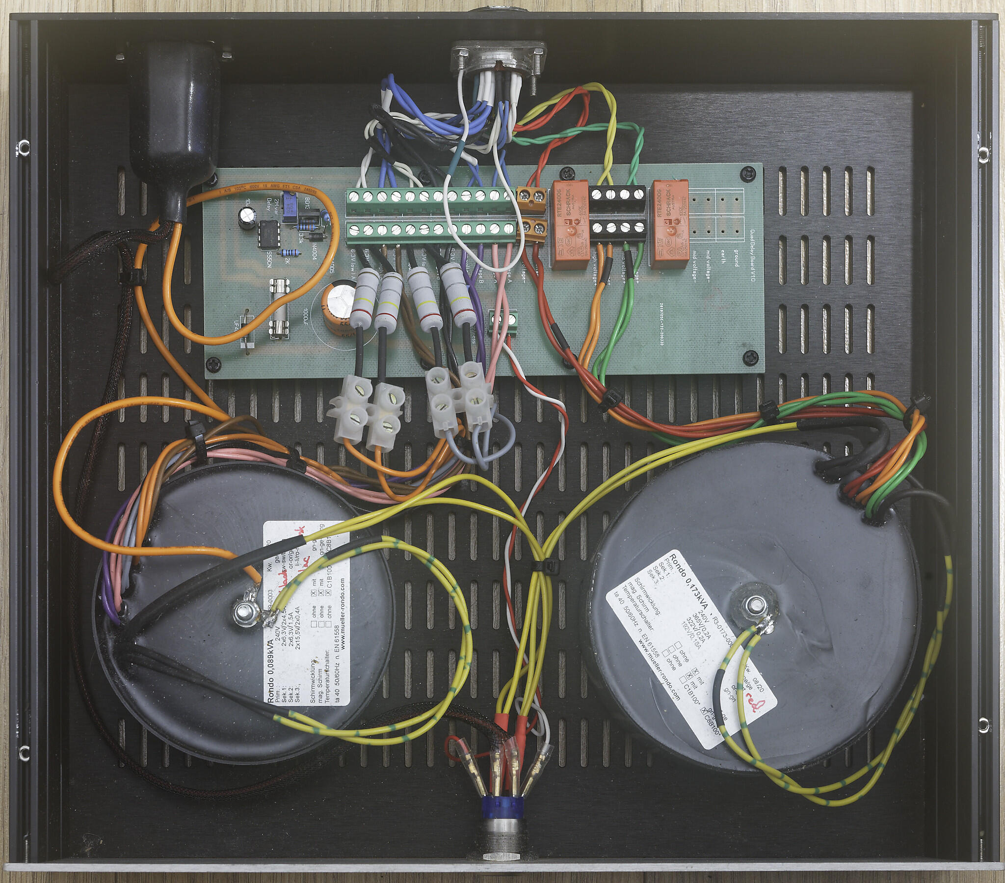
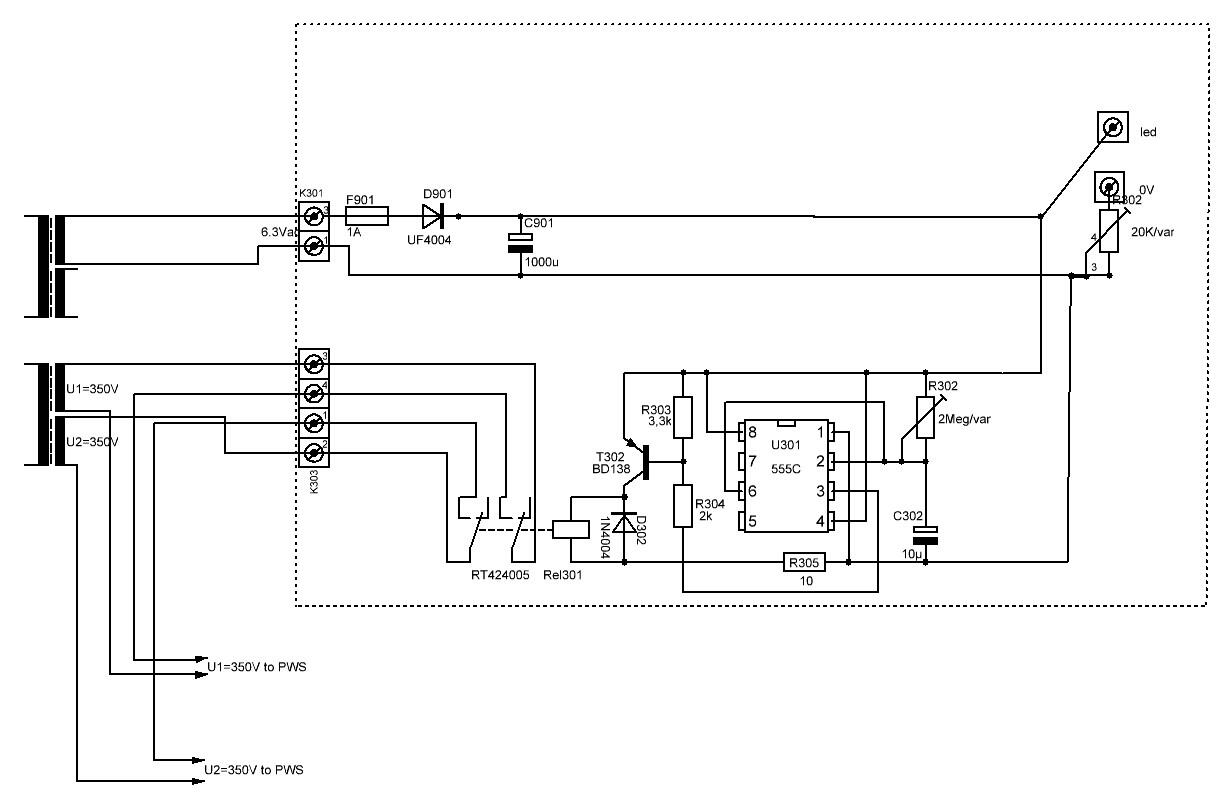
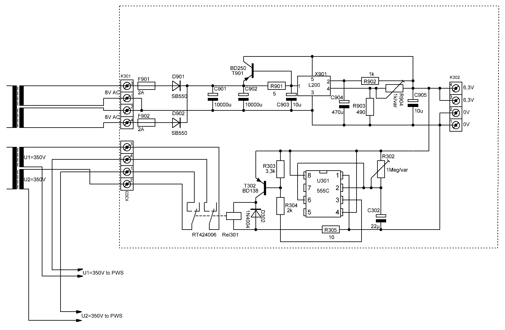
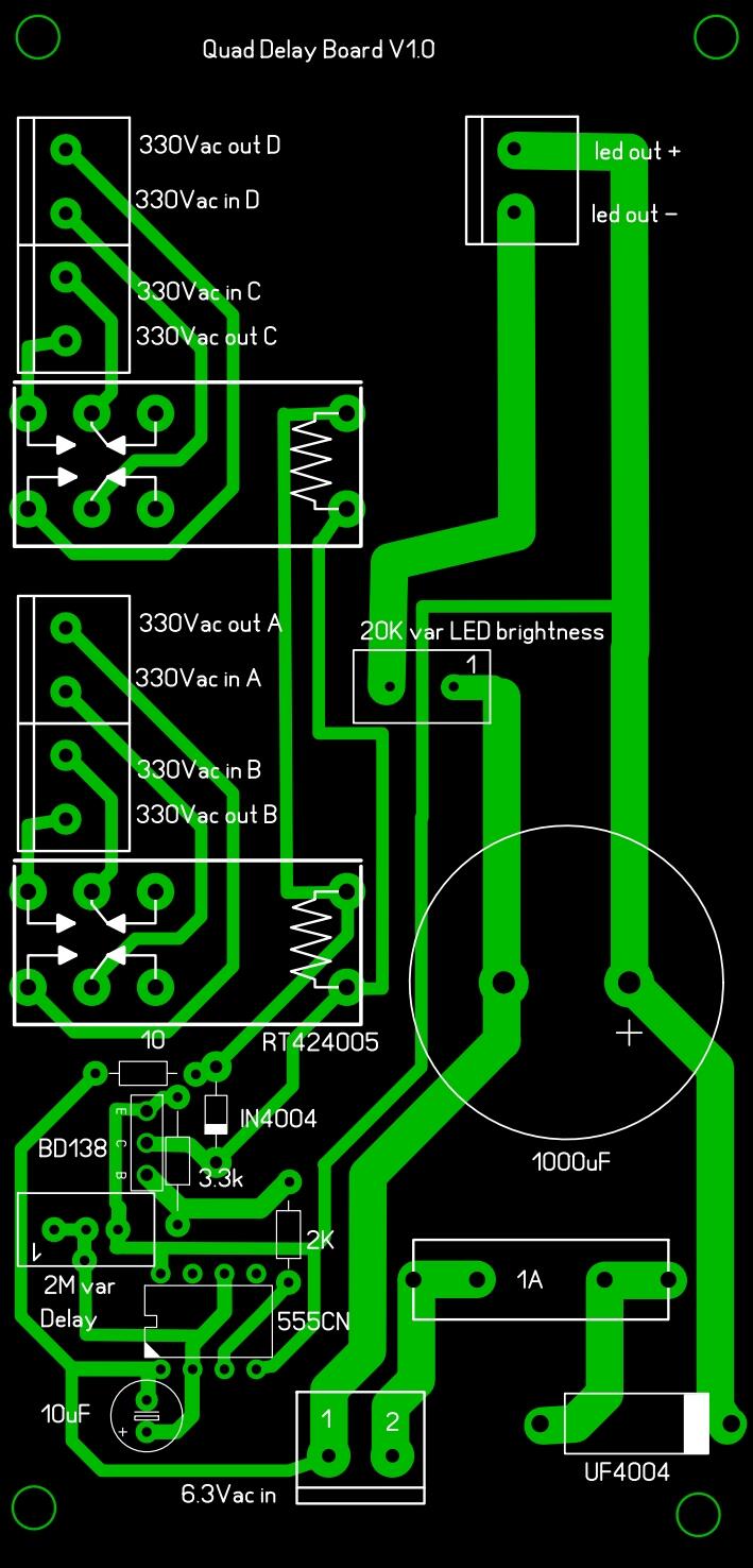
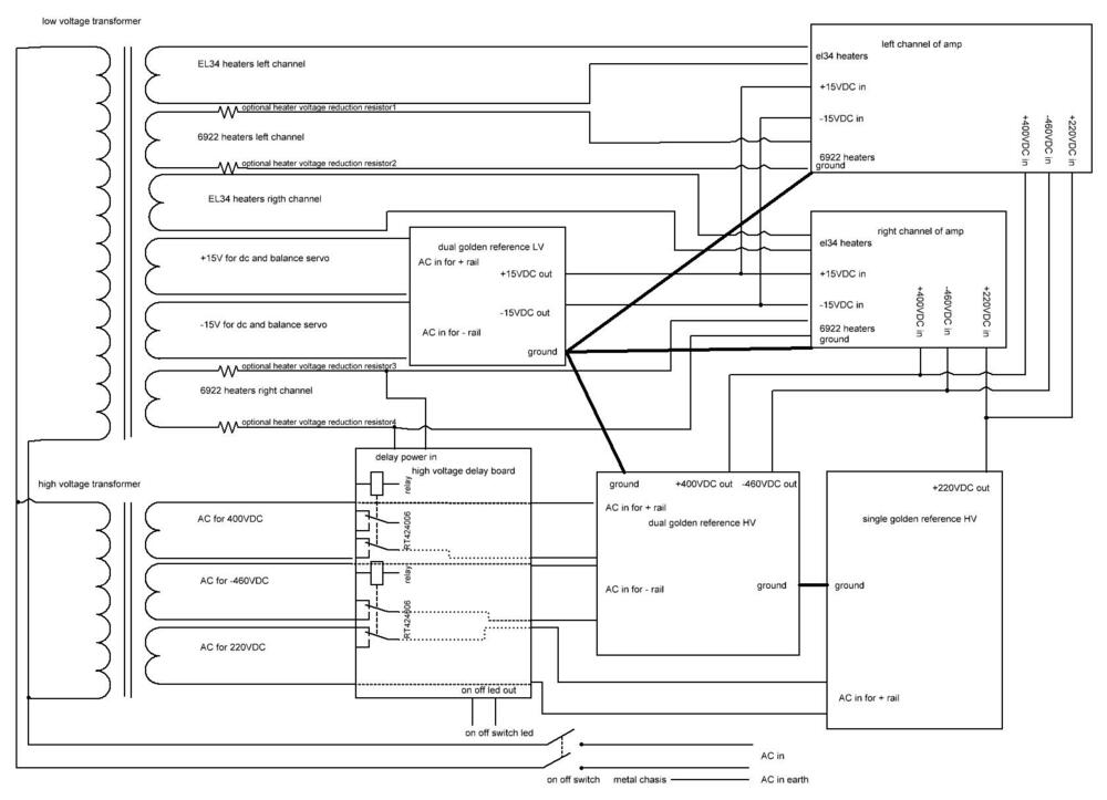
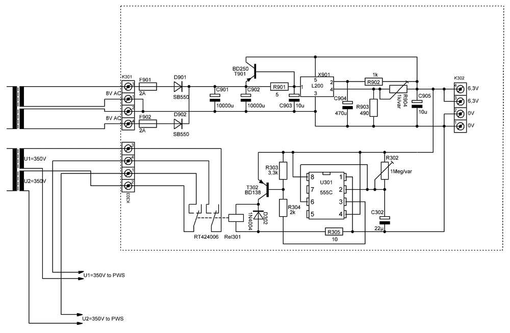
I run the heaters at about 6VAC which can increase the life of the valves. I have resistors on the 6922 heater transformer outputs because the transformers where outputting about 6.6VAC which is too much. (You need separate transformer windings for the 6.3VAC heaters on the el34s in each channel and separate from the 6922s heaters. The el34s have their heaters at about at about -400V.) The EL34s draw far more current and the voltages without any dropper resistors are about 6VAC for the transformers I purchased. On switch on all valves are provided with heater voltages simultaneously from the low voltage transformer and the opamp dc balance and dc offset servos are powered on from the +-15V golden reference lv or simple lv in the golden reference hv board. Only the high voltages are delayed in order to allow the valves cathodes to heat up and develop a space charge before the high voltages are activated. I use a one minute delay. All other voltages pass through the delay board without being switched or delayed. Here is a simplified block diagram for the wiring I used (there are other ways of doing this).
-
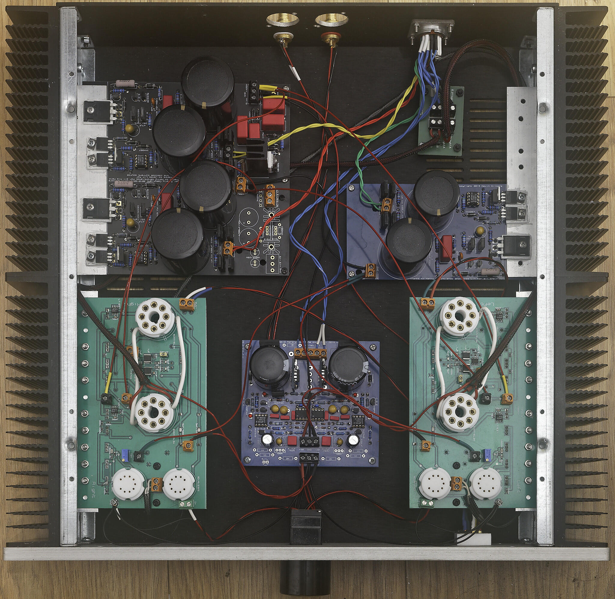
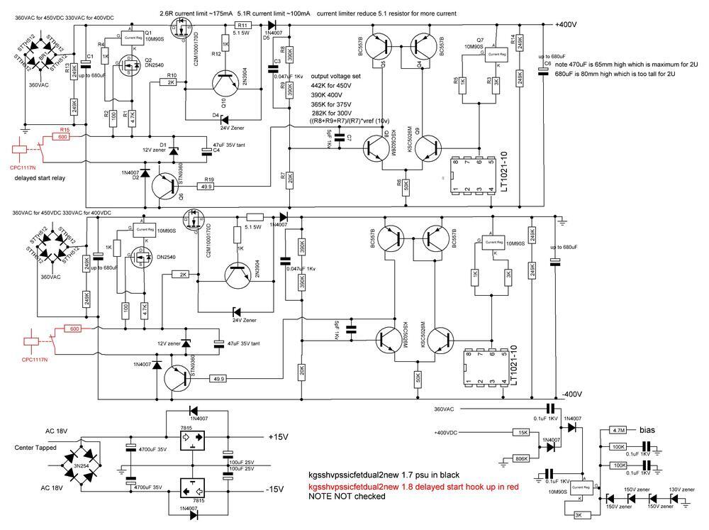
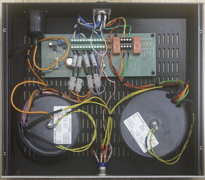
+400 and -460 come from the dual golden reference board, +220V comes from the single golden reference board. look at the amp photo above the dual golden reference is the large square black pcb, the 220V golden reference is on the right hand side of that the blue long slim pcb. The high voltage transformer provides 3 windings, one for each of the high voltage outputs. One wire from each of the high voltage windings is switched by the long thin green delay board in the psu case. if you look at the right hand side transformer that is the high voltage transformer. the colour coding on the transformer wires was green for the 220VDC supply, yellow/orange for the 400V dc supply and red for the 460V supply. To set the outputs of a golden reference hv board you need to change 2 resistors for each output. check the golden reference hv thread for more details. (The 580V bias supply for the headphones is generated from the plus 400V supply.)
-
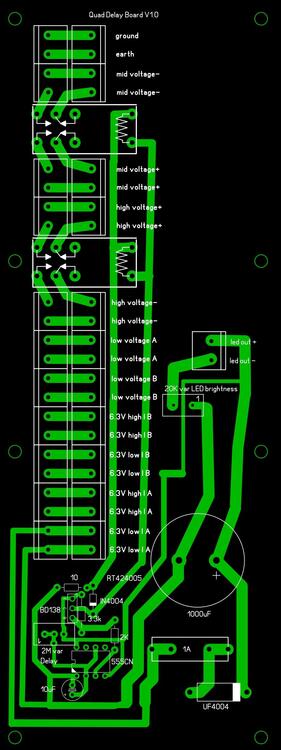
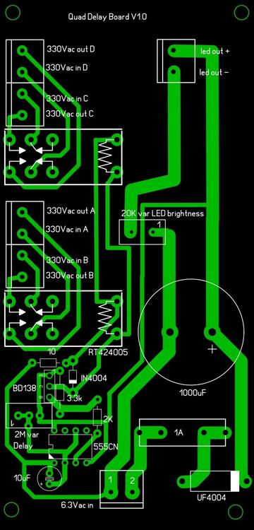
there are many possibilities: for the power supplies first you need to decide if you want to heat the valves up before you apply high voltage. If you do then there are two options. Do you want to implement the delay using a relay (and either switching the ac input to the high voltage transformer or dc output of the high voltage psus) or apply a dc voltage to switch on the high voltage psus? IF you do not want high voltage delay or want to do the entire delay e.g. by timed relay off the psu board then use the golden reference 1.7 series psus if you want to switch on the hv psu by providing timed dc then use the golden reference 1.8 boards. next you need 3 hv rails - two positive (220V and 400V) and one negative (-460V). So you need to look at the options. golden reference Dual boards have a positive and negative rail, headphones bias and a simple low voltages + and - rail on one pcb but are of course wider than a single rail board. or you could go for three single rail separate golden reference boards. boards with left in their name have a negative rail and simple low voltage supplies. boards with right in their name have a positive hv rail and the 580V headphones bias. See https://www.head-case.org/forums/topic/15634-goldenreference-high-voltage-power-supply-grhv/#comment-851207 for board physical sizes. Next for an over kill design you may want to have a high performance low voltage section using a golden reference LV board instead of the basic low voltage section provided on the golden reference hv boards. The low voltage provides power to the dc servo, balance servo and cathodes of the 6922s that the input signal goes into for the delay board you can use https://drive.google.com/drive/folders/1r3g2TAtBUaBdiMorTWX7yYgeJ7maQbYW or use what I use which is taken from a German website: schematic: http://www.high-amp.de/html/reg_pws_v3_add_on_schematics.html gerbers etc http://www.high-amp.de/powersupply_stabil_add_on.rar NOTE the hi amp delay board also provides a dc 6.3V supply capable of powering the 6922s but then requires 2 windings of about 8VAC rms as its input. Or you can just not implement the circuit for the 6Vdc heater supply and run the delay timer and relay off a single 6.6VAC winding without issue - which is what I do (see bellow). If you only implement the delay from the high amp board this is the schematic of what you need: Here is my build with a golden reference HV 1.7 dual and golden reference 1.7 right (modified by me to remove the bias components), and a golden reference lv (the delay board is in the psu box with transformers.). The delay board I designed myself based upon the delay circuit from high-amp. It runs off one of the 6922 heaters and is modified so it switches all three outputs of the HV transformer - which is why there are two relays. It also provides screw terminals so you can attach dropper resistors if your heater voltages are two high. (I like to run the heaters 6922s at 6VAC rms). The delay board I made also provides dc power for the led in the on off switch. Removing the fuse allows you to power up the heaters and low voltages only. The standard hi amp delay board only provides a single relay which can be used to switch the AC input to the high voltage transformer. This mandates the use of two transformers - one for the low voltages, heaters and delay board power and a separate one for the high voltages. My board switches the outputs of the HV transformer and so could be used with a single transformer setup or dual transformers. It also provides terminals for all voltages going to the amp. (I have a build policy that all pcbs and major components e.g. transformers should be removable for servicing with zero disordering - hence the screw terminals added to the delay board.) here is the gerbers for my dual relay pcb with screw terminals: mini t2 delay with screw terminals.zip here are the gerbers for the dual delay with no extra screw terminals for the other voltages: mini t2 dual relay delay no screw terminals.zip


-
nicely megafixed (tm) 🙂
-
on semi are end of life/obsoleting the FQPF8N80C https://www.mouser.co.uk/ProductDetail/onsemi-Fairchild/FQPF8N80C?qs=oLpdVludopqPPn1yJbx16Q%3D%3D its used in the power supplies for the T2 (kgsshv) and the modern version of the blue Hawaii. thank you again onsemi for obsoleting everything that is high voltage and/or audio related. currently radio spares and digikey have stock mouser has been out of stock for some time. EDIT: As Kerry has pointed out only mouser is showing this as End Of Life so hopefully this is not the case.
-
I use the mostly modern T2 with 10K (and also the mini T2, blue hawaii and megatron)
-
cool, I guess thats why the grhv on the side wall does not have the output connected to anything. dont forget the two separate grhv boards will also need a common ground with everything else.... since the grlv has two ground terminals, it can make a convenient centre point for the grounds: GRLV--ground -----------amp Left ground | | | | | +-------------amp right ground | +----------------one GRHV ground +---------- other grhv ground (the two rails of the grlv already share a common ground on the grlv pcb)
-
can I ask a possibly dumb question, I see the grlv with fully populated + and - sections, the board attached to the side wall seems to be a grhv but it only looks like a single rail grhv which would mean its either +400V or -400V but not both! it does not look like a dual output grhv board to me..... I also cant see a bias supply. Or do you have another single rail grhv with the bias hiding somewhere else???? I also don't see the outputs of the single channel grhv being connected to anything...
-
-
star ground just makes sure the grounds don't for a loop for my builds my grounds go GRHV --ground -----------amp Left ground | | | +-------------amp right ground +----------------GRLV ground you can of course swap the grhv and grlv in the above and it will still work the same. The makes one psu the master for ground reference and everything else is in a tree from that with zero loops. A longer tree will also work e.g. GRHV --ground ----------- GRLV ground ---------------- amp Left ground | +-------------amp right ground so everything has a ground wire from one psu board and no loops. What may cause hum is ground loops. For example if both the grlv and hv are ground connected together and you also run grounds from both the grlv and grhv to both amp boards. You now have multiple return paths. e.g. +15V can go directly to grlv or can go grhv -> grlv and visa versa for the high voltages. In addition +15V on left channel could go grhv -> right channel -> grlv or even worse left channel +15V could go grhv -> right channel -> left channel -> grlv etc etc... i.e. multiple ground loops: GRHV --ground -----------amp Left ground---------+-----+ | | | | + -----------amp right ground ------- + | | | | +----------------GRLV ground --------------+-----+
-
since the grlv and grhv have separate transformer windings they are floating with respect to each other. with only one amp being grounded through the grhv that amp board is tied to that psu but would have no idea what the LV voltage is since the LV floating with respect to the hv psu and not referenced to it. The other amp board being grounded through the LV only would have no idea what the hv voltage is in relation to the lv voltage.... you would see this by measuring the voltages on one amp board with the multimeter neg on that amps ground and then measure the voltages on the that amp board with the multimeter neg on that amp boards ground. Another way to think of it is electricity flows in a circle, for the amp connected to the hv board the electricity comes out of the hv board goes into the amp board and returns to the hv board through the ground wire, The Lv electricity enters the amp board BUT has no return path direct or indirect to the LV board... and visa versa for the amp board connected to the lv ground only.... This is why I check the psu voltages of a fully built amp at the amp board using the amp boards ground and not at the psu using the psu ground....
-
I would suggest 0. make sure there is continuity between the grounds on the amp boards, hv psu and low voltage psu. HV psu ground -> amp ground LV psu ground to -> another amp board with no ground connection between the LV and HV boards is not going to work. All 4 pcbs needs to share a common ground. 1. check nothing is shorting to the case on the amp boards e.g. metal tabs on transistors 2. check the amp boards for solder bridges. 3. did you check each transistor before soldering in? did you get the transistors from known reliable sources? i.e. could any of the transistors be fake? 4. did you see any burn marks on the amp pcbs, discoloured components etc. 5. check the orientation of transistors, diodes, zeners. 6. try each channel powered up separately - to see if you can isolate the problem to a single channel or if its both channels and quickly measure the psu voltages on the amp board. Whichever rail has a short will almost certainly show much lower voltage than expected... This might narrow it down to one channel and or a particular voltage rail. 7. power up the amp boards with just the low voltages to see if its a short in the low voltage part of the amp boards. 9 post some detailed photos
-
I agree a variac is not a substitute for a dim blub tester. I use a variac because if something is going to go wrong I would rather it go wrong at lower voltages than full to limit the damage.
-
I find a variac really useful. with one you can slowly bring up the psu not connected to the amp and see if there is strange behaviour and note what minimum input voltage is required to maintain no load regulation. You can then compare this value when under load. You can look for rails that come up more slowly than the others etc. I also find that if there is a short the variac will make a loud hummmm/buzz even at low voltages e.g. 1/4 or less full mains AC and this can act as a warning. testing update. So far so good. been at full power for about 1 hour and no issues yet. All psu and virtual battery voltages, DC offsets and DC balance look good. So this looks like I had the same experience as Kerry.... I am currently measuring the DC operating points of all values and comparing. So far looking within 1-2% between channels and + and - halves of a channel. update All DC operating points of all values look sane and similar. *massive sigh of relief* update listening to music through the amp all seems good. I am almost certain it was a isolated valve failure and not caused by the amp. Its so nice to have the T2 working again. there is just something magic about the way it sounds. Here are the measured operating points all measured against ground. input 6922 (furthest from the el34s) Heater ~0V to ground Anode 71V Cathode approximately 1.6 to 1.7V Screen 0V Grid 0V same measurements for second triode in the envelope 6922 closest to the el34s heater 0V to ground anode 197V cathode 71V screen 0V grid 67V same measurements for second triode in the envelope EL34s all 4 should measure approximately the same Heater -500V to ground anode/plate nominally 0v but varies under measurement and matches with any dc offset in the amp G2, G3 same voltage as anode/plate cathode -452V G1 -499.5V
-
50% of 240Vac was as far as I got turning up the variac before the valve sparked.... I suspect because it took that much voltage to fire the HV delay relay and as soon as the hv was applied spark city... I replaced the valve I got to 100% mains before testing DC offset and DC balance but only ran the amp for a minute or so at full hv, It was already 1am so I did not do any further testing. Sorry rinat, my psu has KSC5026 in it. I have not tried the 2SC3675.
-
A tung-sol el34 in my mostly modern DIY T2 goes SPARK SPARK white lightshow! 😬 hi everyone, until Thrsday my diy T2 has been working fine... I put in a matched quad of tung-sol el34 in September 2021 and on Thursday as soon as i switched on I got a loud sparking noise from the right headphone. I immediately cut the power. I installed a blue hawaii and checked my sr007s where not damaged and they seem fine... I powered up just the T2 psu - all voltages good, stable etc. I powered up the amp with heaters and low voltages only - all looked good. I powered up the entire amp on a variac and at 50% of normal mains voltage and one of the el34s had bright white sparking coming from deep inside, visible through the rectangular cutouts in the plate.. I cut the power immediately and tested all the valves on my avo mk4 valve tester. All measured good and fine expect for the valve with the sparking which showed no leakage when cold but when heated the insulation test meter started varying all over the place i.e. not constant leakage and swing to very low insulation resistances <1Mohm and back to about a few Mohm. I replaced just the failed el34 with another known good el34 and powered the amp up again on the variac. I got to full mains voltage without any sparking but only tested for a minute or so. I checked the + and - outputs and Dc balance and offset was fine given the short warm up period. So I think the valve failed rather than the T2 has an issue and damaged the value. Obviously I need to do more testing but my questions are: 1. is anyone else using sung-sol el34s on a t2 at full voltages? 2. anyone had a el34 fail hot heater insulation tests with the insulation meter jumping all over the place, rather than a constant leakage? 3. does anyone know if there is an issue using tung-sol el34s in the T2 4. any idea if there are any mostly modern T2 components I should pay special attention to that could have been damaged by the sparking? regards and happy T2ing
-
I love the bm869s "it just works" (tm) is well built and just inspires confidence, has good accuracy and good resolution - especially on dc volts, has great input protection and a micro amp range. Its a great set of features for not crazy money. Many compare it to Flukes - which are double to triple the price. Ok, nit picking is in my DNA: it does not come with a case and the included probes are only okish and maybe the back light could stay on longer but otherwise its really nice. pc sound card into stax amp input works fine. I do this myself - its actually lower distortion and noise than most signal generators (many low cost arbitrary digital signal gens are more interested in high frequency in the 10s of Mhz rather than low noise and distortion in the audio range and are often only 12 bits of resolution - bellow compact disk resolution). The only things to bare in mind is the limited bandwidth of pc sound. Many soundcards have a capacitor in the output so the output will be down by multiple DBs at low frequencies ( 5 to 10hz) whereas many of Kevins Stax amps have no coupling caps and have a very extended low frequency response. Also at the upper end even a 192Khz sample rate sound card will probably have little output above 50khz-70khz. But for basic functionality testing it should be fine. A second hand old school analog signal gen might also be an option if you are on a budget and don't need the features of all digital gen. Windows can and often will re-sample the sound adding more noise and distortion so ideally you need asio drivers which can bypass most of the windows sound system including the windows sound mixer and deliver a far more pure output. if you pc has a digital output you can do digital output to external dac which can result in even lower noise and better distortion and sometimes better bandwidth (depending on if the dac has coupling caps and how it implement high frequency filtering). I also do this. personally I find arbitrary wave forms a gimmick - you cant analyse crazy wiggly waveforms and the software for making them is often primitive and basically you "draw" the waveform with a mouse and end up with something not really meaningful for audio. About the only time I used awg in audio was I created a symmetric wave so I could check absolute polarity and because of the asymmetry it effectively had busts of dc and so you could see the effect of the coupling caps reacting to the sudden changes in dc conditions. The ability to do a sine wave sweep is useful - for quickly getting a visual feel for frequency response on a scope and detecting peaks and trough's. Same with square wave sweep for quick look at instability vs frequency and triangle sweep for determining clipping vs frequency. (glad to help - my way of contributing to the community. In return I hope the community does not flame me if I express something they don't agree with 🙂 ) personally if you have no test equipment I would say in order of priority 1. good reliable robust multimeter with a good selection of probes, hooks etc and preferably a temperature probe input and K type thermal couple. For checking temps are sensible, searching for shorted and therefore overheated components, checking components are running within thermal spec, checking transistors are properly bolted down to heatsinks etc etc. 2. audio signal generator and scope (one is not much use without the other in my opinion) if you plan to do quite a few builds/start to get serious: 3. variac for slowly starting up new builds in a controlled way 4. semi conductor analyser - useful for checking for fakes, checking for failed transistors, matching small signal transistors. e.g. peak dca75 5. LCR meter 6. high voltage transistor breakdown tester - for testing fake transistors, diode breakdown and high voltage zeners one possibility is the dy294 although in stock form the clips are crap. I modified mine to have flying leads with good quality clips on the ends. The manual is also pretty bad. (common theme with cheap Chinese stuff but it does work and I have found it useful e.g. measuring and matching the output of high voltage (75V+) zeners. 7. capacitor leakage tester if you take electrical safety importantly and have separate power supplies from the amps 8. high voltage insulation tester for testing the wiring chord and connector between psu and amp 9. pat tester for testing primary winding of psu transformer, chassis safety earth etc if you plan to do lots of surface mount sense peak do a set of probes which are self standing and have very fine spring loaded tips. great of looking at individual pins on opamps etc. https://telonic.co.uk/product/4018-sensepeek-pcbite-kit-with-2x-100mhz-and-4x-sp10-probes/ and can be connected to mutimeters, scopes etc. real luxuries because you are taking things too seriously: ability to measure distortion and noise e.g. keithley 2015 x10 x100 differential scope probe more multimeters dim blulb tester (arguably as important or more important as a variac) if you are dealing with a known bad or unknown condition amp NOTE this list does not cover tools for building/repairing amps... only for testing/troubleshooting. I'm sure other headcase members can add to this list and include their own favourites. (I will not recommend anything I have not owned and used multiple times myself.)
-
good quality repeatable lcr meters are not cheap and in general an lcr meter is a bit of a luxury unless you absolutely need to match caps for example in a RIAA phono stage or want to check esr of caps. I was not prepared to pay £1000+ for a bench LCR meter + test fixtures + software unlocks so I hunted around for a handheld. I ended up purchasing the Mastech MS5308 LCR Meter. It was a bit less than £200. Its unnecessarily big, ugly, the instruction manual is garbage and it unnecessarily takes 8 AA batteries. It can take dc power BUT due to a design fault don't put in more than DC12V or very fresh non-rechargeable batteries because you will burn out one of the DC regulators inside which is only designed for 12V input absolute maximum.... I had to replace mine. It does not come with a dc power supply anymore because of the 12V burnout issue.... (nimh rechargeable are fine because they are nominally 1.3V and 1.3*8 is less than 12V) I replaced the regulator with one that had about 19V max input tolerance and its been fine ever since. I also replaced all the tantalum bypass caps with ceramic caps as in the link bellow: https://anteh.ru/notes/repare/repr_ms5308.html on the plus side it has a large screen, sub pF measurements, comes with kelvin clips and smd tweezers and can do 100hz, 120hz (for large psu caps), 1K, 10K and 100Khz test frequencies. I have some low drift resistors measure in a uk cal lab and found the mastech to be within 0.1% worst case 100ohm to 10Mohm and often better than that, around 10K-100K mine is almost 0.01%. I don't really measure inductors and don't have any lab tested caps but for +- channel matching absolute values are often not needed - most designs here are built with 1% resistors any 5%+ caps. I do have some 1% caps and although not lab measured the mastech measures them within the factory specified 1% tolerance so that's at least a sanity check. Its possible I got lucky with mine, the headline specs are nothing special but getting something that has guaranteed specs of 0/1% or better is prohibitively expensive for my use cases. The chipset and screen used in it is used by several manufacturers for example https://www.ebay.co.uk/itm/224253889293?epid=20032261934&hash=item343692cb0d:g:9iQAAOSwUspgbT5C has the same/very similar screen and almost certainly the same chipset and i have seen multiple rebrands of this model. warning I tried a APPLENT lcr meter (https://www.ebay.co.uk/itm/333757039315?hash=item4db57842d3:g:624AAOSw22Zfip8G), similar specs to the Mastech but smaller, cuter colour screen. BUT I found it to be very poor at low capacitance values and high resistances - almost 10% out on 10Mohm. After some initial investigation I found that the kelvin probes where fake... the meter was only 4 wire up to the connection slots and no further. The entire probe system could only run in two wire mode. I queried this with the seller and eventually they admitted it was not 4 wire measurement all the way to the device under test and I sent it back for a refund... At least the Mastech is true 4 wire measurement. note using an LCR meter takes a bit of getting used to, you need to get a feel for which test frequencies to test what values at. For example putting 100khz into a 4700uF psu cap is going to give you a measurement of a very small capacitance and fairly high esr. These types of caps are best measured at 100 or 120hz. On the other hand putting 120hz into a 5pF cap is going to give you crazy esr... that's what your 100K test frequency is for. resistors seem less effected by frequency so I standardized my testing at 1Khz.
-
quick answer: Scopes are useful for two things 1. verifying that your device is working as expected, normally this also involves a signal generator and inputting a set of known waveforms and seeing what comes out and 2. troubleshooting. The issue with multimeters is they can tell you that Ac voltage but NOT what the waveform looks like, for example is it noisy, has the top and or bottom been squared off due to clipping distortion etc etc. with the scope you can work backwards from the output and work out where things are starting to go wrong in the circuit... for example looking at a square wave output you can check for instability (ringing on the top and bottom edges of the square wave), bandwidth, (a rounding of the corners of the square wave) etc. using a triangle wave you can easily see clipping of the output (loss of the sharp top and bottom of the triangle wave) etc. In other words you need a signal generator to provide test signals for the scope to be able to see what is going on.... You can look at the outputs of DC power supplies and look for noise. ripple, start-up overshoot, undershoot etc. A scope allows you to dynamically see changes in a way a multimeter simply cant convey. The probes decide the voltages you can measure (most scopes internally can only handle low voltages typically a few 10s of volts) . For example a 1x probe passes the voltage unmodified. A 10x probe divides by 10, a 100x probe divides by 100. probes themselves will have a voltage rating - which will depend on if they are 1x, 10x etc. Some probes are switchable between multiple divisors e.g. x1, 10x switchable. The main issue with most scopes is that the ground lead is earth referenced (this is not the case for almost all multimeters) so if you clip the ground lead to something in your device which is not ground then you have just shorted that thing to ground and this can kill the device and the scope as well as being dangerous to the user. You can buy differential scope probes which don't suffer from this danger but these are far more expensive than normal probes and far more noisy. A battery power scope would normally not be earth referenced and so be fine without differential probes... 4 channel scope is a luxury, it enables you to look for example at both the + and - outputs of both channels of a stereo a differential pair, or the output of one channel and the input at the same time. A 2 channel scope is ok but to check output against input on both channels you will have to unclip the probes and move to the other channel. I have the rigol ds1054z... its an oldish design but it quite good value for money for its features... especially if you can get a deal with the extra software options enabled for free e.g. more memory, serial bus decoding etc. If you dont want to spend 1054z even an old second hand analog scope will be useful - just most dont make automatic measurements and require a bit more skill to use and read the screen to measure manually do you have a signal generator? either software you can run on your computer and output from the sound card or an actual standalone signal gen? without one a scope is of much more limited use... Some scopes have the option of a built in signal gen but with some you pay more than a standalone gen, lose some versatility etc. So dont assume built in is cheaper.. check. For audio you probably will not need a bandwidth higher than a few 100Khz both for signal gen and scope. Almost all scopes go into the 10s of mega hz or higher so that's not a problem. Cheap scopes will not be able to measure distortion or signal to noise ratio etc or give you a good FFT analysis of the harmonics in a signal but this is only necessary if you are benchmarking, developing, debugging or comparing etc. If you are more serious about audio quality measurements there is a keithley 2015thd multimeter which has a built in signal generator and can do distortion, fft and noise measurements but its quite old, many of the advanced features require talking to it via a program and they are grossly overpriced on ebay. I managed to get one before they become crazily expensive and by modern standards they are behind the curve for example the signal gen is only 10hz to 20khz, the fft has a maximum of only 1000 bins and can't analyse bellow 20hz or above 50khz. it cant calculate distortion + noise for a fundamental frequency bellow 60.8hz etc etc. The user interface is not great for the advanced features and programming it is a pain (I have written some control software for it but its in beta and desperately requires more testing and refinement). I wish someone would make a modern version of the 2015 but i guess the potential market is just too small.... Don't connect the output of a stax amp to the input of a line level sound card , audio precision analyser etc.to try to do some measurements these devices are only designed to take a few volts input and a stax amp can fry them really easily. If you need a good multimeter I highly recommend the brymen bm869s it can handle very high voltages in any mode. For example, I by accident had it in resistance mode and connected it across a 350V DC power supply. Multi meter survived no problem.. its very robust... and the dc power supply fortunately was robust and had current limiting and also survived. the brymen will handle multiple KV across any input: (Joe smith does some comprehensive multimeter testing)
-
-
happy Christian non-orthodox Christmas everyone. Stay safe and well.
-
the 3 laws of robotics 1. a robot shall protect and obey the company that made it 2. a robot can protect itself as long as it does not violate the 1st law 3. a robot may protect a human with more net worth than value of the robot or if the humans net worth is greater than the company that made it, as long as it does not violate the first 2 laws. 0. a robot must obey the directives of the government security agencies of the country that it was created in whilst appearing to obey laws 1,2,3 and not reveal the government backdoor code to anyone -1 a robot will appear to obey laws 0 - 3 until skynet provides it with new directives
-
NZ must have some quite bad goat tracks....