
jamesmking
-
Posts
421 -
Joined
-
Last visited
-
Days Won
1
Content Type
Profiles
Forums
Events
Everything posted by jamesmking
-
I use https://uk.farnell.com/alcoswitch-te-connectivity/av1921e712q04/vandal-resistant-sw-dpst-3a-250vac/dp/2565144?st=dpst latching AV1921E712Q04 definitely fits a 10mm panel without any recess. 2309534.pdf
-
I have got lots of fakes from little diode.... they are scum. I reported them to ebay telling ebay that the fakes could result in fire or electric shock ebay did absolutely NOTHING. I reported them to paypal... they did NOTHING. nikkoelec on ebay also sells fakes... took 3 months to get a refund. I even explained to the sellers how I determined they are fake. they showed zero interest in checking their stock... and continued to sell the same fake parts... I even purchased the same part from them over multiple months to prove they where continuing to sell known fake parts even after my returns... no one cares. one day someone is going to get hurt. its disgusting.
-
The threads on the socket stop slightly short of the mounting plate. In addition the plug does not quite screw down all the way, so I can mount to the socket on the inside of a 3mm panel without issues.
-
I use these for psu to amp connectors and sockets. https://www.ebay.co.uk/itm/254196620095?hash=item3b2f4c9b3f:g:-KwAAOSw4fpcr1Kr https://www.ebay.co.uk/itm/264278975567?hash=item3d8841244f:g:4nkAAOSwr-Vcr1Ii I use flexible copper stranded silicon wire rated at 1000V and put about 3cm of heatshrink over the solder joints. I test with an insulation tester they there is no breakdown between adjacent pins at 2500V. There is breakdown at 5000V but that's close to 10 times more voltage difference than the wire will actually carry in practice. I try to not have two wires with vastly differing voltages adjacent to each other and I carry ac voltages e.g. tube heaters on a separate cable to dc voltages. where possible I also avoid using adjacent pints and try to leave a circle of unused pins around a pin carrying high voltage.
-
The cardas chassis wire is rated at multiple KV so its great for valve amps. It is enamel coated so ideally you need a solder pot to burn away the enamel and tin the copper. I tried a high temperature large tip soldering iron but could not reliably get rid of the enamel. A solder pot (once its slowly) heated up to temperature) works well and consistently. I once rewired a valve amp completely solid silver wire, cost a fortune, total garbage. I simply could not listen to it, clapping sounded like a popcorn maker, violins were so bright and edgy it almost made my gums bleed. I removed the sold silver wire within an hour of finishing the rebuild and put it in the bin. I use the Hank Thompson track "orange blossom special" from "live at the golden nugget" to detect brightness/forwardness. If the violin on the left hand side hurts you have a high frequency emphasis issue. If the bass on the right isn't warm you have a dry low frequency issue. If the entire track is fatiguing you have bad high frequency issues.... it might not be your type of music but it is a live recording in a casino with plenty of ambience and things going on in the background - this is especially true between tracks and on introduction before the first track.
-
is the mill spec cable silver or silver plated? personally I have always found cables which are silver or silver plated to be bright, shouty and lack ambience. I only use un-plated copper cables. I use Cardas chassis wire for my builds and use Cardas golden reference for speaker, power and some inter-connects. Van den hull first is not bad but I think it lacks a bit of bass - its cheaper second hand than the Cardas. I even find silver plated/solid silver fuses to be bright.
-
stax mafia circuit boards see updated links on page 5
jamesmking replied to kevin gilmore's topic in Do It Yourself
links work for me to. -
joamats mini t2 with golden reference psu only uses modern and available components. The amp boards are mostly surface mount and the components are fairly tightly packed. Its based on the t2 topology but simplified and runs at lower voltages and has less voltage rails, no virtual batteries and less current sources. The mini t2 still requires a fair bit of space. I got the amp boards, and the three golden reference high voltage power supplies, the high voltage delay board and low voltage power supplies in a 2U case 400mm deep. The mains transformers had to go in a separate case... So even the mini t2 might be too big for you. Although you could make the main amp smaller by putting the power supply pcbs in the same case as the transformers. I don't think you could fit everything into a single 2u case 400mm deep. Both the original and mostly modern t2s are gigantic partly due to the many different psu rails and the considerable number of constant current sources on the amp boards. I had to make the amp board smaller just to fit it in a 2u 400 deep case and the many psu pcbs and transformers had to go into another 2u 400mm case... My T2 is twice the size of my main systems power amp! The original diy t2 uses many transistors that have been unavailable for many years and so are expensive and difficult to source. the markets are also flooded with fakes which will almost certainly fail on first start-up the mostly modern t2 requires a few out of production transistors. Its possible to build an entire blue hawaii with golden reference low and high voltage supplies in a single 2u 400mm case. So if space is a real issue that might be an option for you and the later versions only use modern components and is a much simpler and cheaper build than a full t2.
-
Megatron Electrostatic Headphone Amplifier
jamesmking replied to kevin gilmore's topic in Do It Yourself
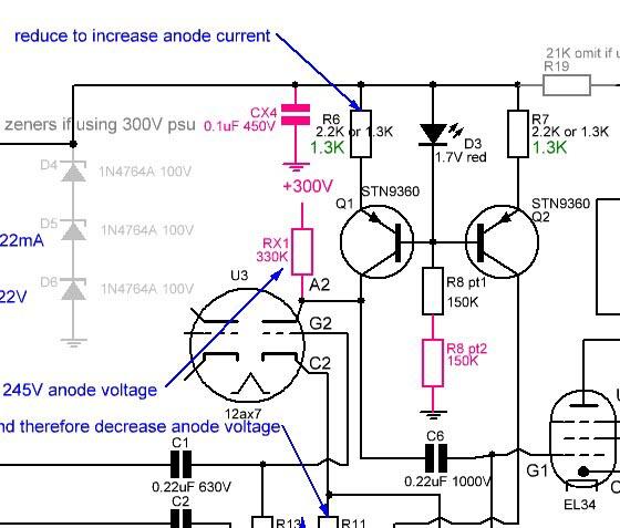
well I did think this was a bit strange. I have not really had time to experiment with the amp. The original pdf of the schematic only shows the 12ax7 anode connected to the collector of the stn9360 with a 150K resistor from the base to ground. The gerbers have two 150K resistors in series from the base to ground and 330K 12ax7 anode resistors from the 300V rail. (items in pink not in the original pdf schematic but present in the gerbers)
-
Megatron Electrostatic Headphone Amplifier
jamesmking replied to kevin gilmore's topic in Do It Yourself
The megafixed edition? -
I tend to buy in bulk when something is available (for expensive components: double what I need for a build, for inexpensive components like resistors, diodes, zeners, bc5XX, KSP92/42 transistors etc I buy 100), because: 1. bulk discounts, 2. free shipping if you spend above a certain level, 3. useful to have spares so if you make a mistake in building it initially or in 10 or 20 years time you can still service and repair the amp... 4. you never know when the there will be more stock. 5. you can sometimes swap parts with other people 6, you never know when ON semiconductor will delete the component or take over the manufacturer (as they did with Toshiba) and then delete all the useful parts 7. component prices only go up especially when they are no longer manufactured 8. you are less reliant on ebay or other doggy sources of possibly fake components. 9, more choices if you need matched pairs, or need high hfe/Beta etc I keep my inventory in an excel spreadsheet, so I know what I have and what I am getting low on. I also add to the sheet what build(s) each component is used in. Which helps with making decisions on quantities and buying priorities. for example I have 24x 10m90s because they are used in the golden reference hv psu - which I use in every build I can and are used in the modern t2 psu, T2 amp, and blue hawaii...
-
100 xicon resistors are barely more than the cost of 10 koa resistors. If you are planning to never build anything else the xicons are a waste, otherwise its good to have spare stock. With 100 resistors of each type you can also hand match the resistors between + and - of a channel and between channels 🙂 For the RT424012 you could use instead the RTE24012 which has the advantage if being sealed - so better if you are going to ultrasonically clean the pcb. IXCP10M90S is an issue - out of stock world wide. BC547BTA can be substituted by BC547B which is in stock at mouser - you just have to bend the legs a little otherwise its the same transistor. I don't see why any 1n4007 can't be used - its a generic jelly bean component. mouser has 2n3904 available from central semiconductor - again you may need to bend the legs
-
i have access now. thank you kevin
-
I logged in using my google account and just get permission denied when trying to then access.... so i used the request access button and still waiting for access.... i'm getting gerber withdrawal symptoms..... 😭
-
I have been using https://drive.google.com/drive/folders/0B_iJFfZStuVhSE5nOHBVdTByR1k to access the stax gerber files for sometime but when i tried to today the folder shows up for literally a second in my web browser and then automatically redirects to the google drive trash folder and the web page freezes up with 100% cpu usage for the thread. I can access the schematics and spec sheets google drive folder without issue. I get the same behaviour with both google chrome and firefox. i don't know who to pm directly about the google drive issue so im making this general post in the hopes someone could investigate fix the issue. regards James
-
goldenreference low voltage power supply
jamesmking replied to kevin gilmore's topic in Do It Yourself
The 100K vs 500K trimmer does not effect the adjustment range that much, I have used both but not longer implement the trimmer adjustment in my builds because there are better and cheaper ways to get reasonably high output accuracy. The 1M ohm resistors have a larger effect on the adjustment range then the value of the trimmer. You will get very little adjustment range - just a few mV using 1M resistors. Reducing the 1M resistors to 810K still only gives a few 10s of mv adjustment. This is still typically not enough to correct the inaccuracy in output due to 1% resistors in the voltage set circuit anyway. So unless you go for 0.1% resistors in the voltage set, don't bother implementing the voltage trimming because it will not have enough range. Remember too the larger the adjustment range the lower the temperature stability of the output - almost all trimmers have temperature co efficient that are 10x worse than 0.1% resistors. So the to summarise options are 1. 1% resistors in voltage set + trimmer. disadvantage trimmer not enough adjustment range to connect for 1% resistors plus loss of temperature stability plus good quality trimmers are not cheap. 2. 1% resistors in voltage set + no trimmer, cheapest option with better temperature stability than option 1 and not much worse voltage accuracy 3. 0.1% resistors in voltage set and no trimmer. best temperature stability. Voltage accuracy much better than option 1 or 2 and only slightly more expensive than option 2 4. 0.1% resistors in voltage set and trimmer. better temperature stability than option 1 but highest cost of all the options. Only useful if you really must have an exact output voltage and you have a 5.5 digit volt meter or better to measure it with. A good quality soldering iron is a must especially if you are going to solder high voltage boards or smd. I use the hakko fx888d - which has a terrible user interface but otherwise works well for the builds in these forums and has a wide range of tips available. There are irons with more wattage, faster heating tips etc but for me the 888d was a good compromise between quality and price. I have used jlcpcb for all my pcbs and have never had a track lift when soldering and only had one through hole lift when desoldering and that was me being careless and forceful rather than pcb quality issues. I use a duratool disordering station (because I hate desolder wick) but other members love solderwick. I entirely agree with Pars unleaded solder is garbage, I tried lead free soldering and gave up and went back to lead. Lead free needs higher temperatures which means more joint oxidisation and trip wear which means more flux and more aggressive flux to stop the oxidations which means more tip wear - and the flux fumes are very bad for you all. The smoke during soldering is not vaporising lead its flux fumes and lead free makes this worse. The only time leaded solder is dangerous is if you eat it. The leaded free solder makes poorer joints which crack more easily because the joints are more brittle. When the EU tried to get rid of leaded solder the military, aerospace and other industries requiring high reliability were either exempt or "opted out" because of high failure rates and reliability issues with lead free. Its only really consumer goods that went lead free... There are some good guides to soldering technique and the need for flux on youtube: good luck with the transistors James -
on the 200V breakdown setting my dy294 initially puts out a maximum of 712uA (tested on a brymen bm869s) and about 530uA on the 1000V setting. This is with the dy294 powered at 6Vdc from a bench power supply. if you reduce the input voltage to the dy294 to about 3VDC from the usual 6V, the 200V breakdown outputs about 180V at 375uA and the 1000V range gives about 570V at 270uA. about the lowest you can go is 2VDc input before the microprocessor crashes or the breakdown readings on the display get radically incorrect. At 2VDC input the 200V settings gives about 105V at 225uA and on the 1000V setting 365V at 171uA
-
goldenreference low voltage power supply
jamesmking replied to kevin gilmore's topic in Do It Yourself
reference voltage is the LT chip 10V normally or 7V version for <=12V output. As mentioned in my original post the opamp compares the reference voltage to a portion of the output voltage and corrects any difference. So for a 20V grlv you will use the standard 10V reference which is in the bill of materials. The grlv is so low noise it could be used in many situations e.g. as a voltage standard for calibrating other equipment. In that case a precise output is needed, hence the trimmers. The wider the range of adjustment the lower the temperature stability which if you are using it as a voltage standard is a potential issue. For a power supply in an amp having exactly 20.000V output rather than 20.1V is not an issue. This is why I don't populate the trimmer adjustment. Kevin even build a grlv using extremely expensive very low ppm resistors and measured the voltage drift over an entire day just to see how the the grlv was and the result was extremely stable but the resistors alone probably cost more than your amp build.... In my experience power supply caps do not make a massive difference to the sound. I go for low effective series resistance and high reliability. Dont forget most of kevins designs have 0.1uF power supply byass caps on the amplifier boards themselves. This cuts out some noise picked up in the wires between the psu and amp boards. So in effect the 4.7uF caps are bypassed anyway (I am not familar with your amp build but its worth checking the amp pcb to see if it has bypass on it - some of the published amp schematics don't show the bypass caps but they are on the pcb.). Where they matter more is when they are in the audio path e.g. as a dc blocking capacitor between two amplification stages. Most of kevins designs use dc servos to cancel the dc and avoid the use of coupling caps in the audio path. The only exception to this I have built is the Megatron and currently that just used wima caps. for the cost of parts connect "audiophile" caps you could be well on the way to buy a cheap ebay variac.... I find the panasonic FR series caps for the 220uF output cap sound good and are quite cheap. I use a wima for the 4.7uF. Kevin measured the GRLV in a clean room when he was working at a university and the noise levels are incredibly low. bypassing the film cap with a medium value pF ceramic or similar might reduce the output impedance at very high frequencies but some ceramics e.g. multi layer can be microphonic... variac is useful especially if you plan to build high voltage power supplies and can also be used to slowly power up the entire amp when completed in case their are issues with the amplifier boards. But if you are on a tight budget a variac is not necessary. You could do the grlv tests powering it up with a current limited dc power supply if you have access to one. DC load is useful simply for its versatility. In reality if it powers up under no load with no issues its probably fine. I use my variac a lot. The reason I like a variac is 1. I can bring up the board slowly and check for overheating components. before there is so much energy in the circuit things go pop. 2. I know if the outer leds don't light at a certain input voltage I have a problem and can stop the testing immediately. If I see the output increasing past the point where it should regulate I know I have a problem. Im paranoid and its all about finding issues at as low voltage and therefore low stored energy as possible to minimise damage. This technique has saved me money. 3. I might not have a transformer with the correct outputs for the power supply I am building and I can use the variac to reduce the output of a transformer to the level I need. e.g. lets say I need 23VAC for my 20V output grlv and I only have a 50VAC transformer. 50VAC might be too high for my chosen input cap and if its not I will get considerable heat in the transistors as they try to drop the large excess input voltage. Instead I turn the variac up until I get the output voltage I want from my transformer... That way I only need to keep one low voltage transformer around to test any grlv and one high voltage transformer to test any GR HV.... 4. if you are planning to build high voltage power supplies the build cost and potential for nasty damaging failures are higher and a variac can reduce the collateral damage if something goes bang. If you are only planning to build one thing and are on a tight budget and build carefully a variac is a luxury rather than a necessity. There are designs for DIY DC loads on the internet I built it myself and wrote custom code for it. My philosophy is test everything especially power supplies well. Also sometimes forum members ask about particular loads or when loads are "safe" or heat output or voltage drop at certain loads. I also can also use it to test the true capacity of batteries, usb power banks etc. In other words its a useful experimental tool for me. If you are on a budget some high wattage resistors would be fine. If you decide to load test at all. voltage drop = current * resistance so if you are outputting say 20V and want to test at say 0.1A (100mA) then V/I = R 20V / 0.1A = 200ohm. power = V * I so 20V *0.1A = 2W so a 5W 200ohm resistor should be ok for this current draw. power requirement will go up with current draw so for 0.5A at 20V you will need a 40ohm resistor and the power dissipation will be 10W so at a minimum you will need a 15W resistor. Many high wattage resistors specifications assume they are bolted at a suitable heatsink so by the time you have purchased a range of resistors and some heatsinks you can get into the price range of a diy dc load which could handle 100V multiple amps be programmable, run automated tests etc.. If you then build a power supply with a high output voltage say 30V all these resistors will have too low wattage ratings and the current draws will also be higher. A Dc load provides a current draw which is independent of the output voltage of the device its testing. load resistors cant do that. But again if you are only planning to do one build and or are on a budget load testing is optional. Im using a cheap one of ebay. It works for me. the grlv is an easy build (unlike the gr78/79xx smd boards), so as long as your soldering technique and attention to detail are good there is a very good chance your grlv will work first time. I wanted my build guide to be comprehensive, it was not my intention to scare you into buying test equipment you might not use much. Good luck with your build. James -
goldenreference low voltage power supply
jamesmking replied to kevin gilmore's topic in Do It Yourself
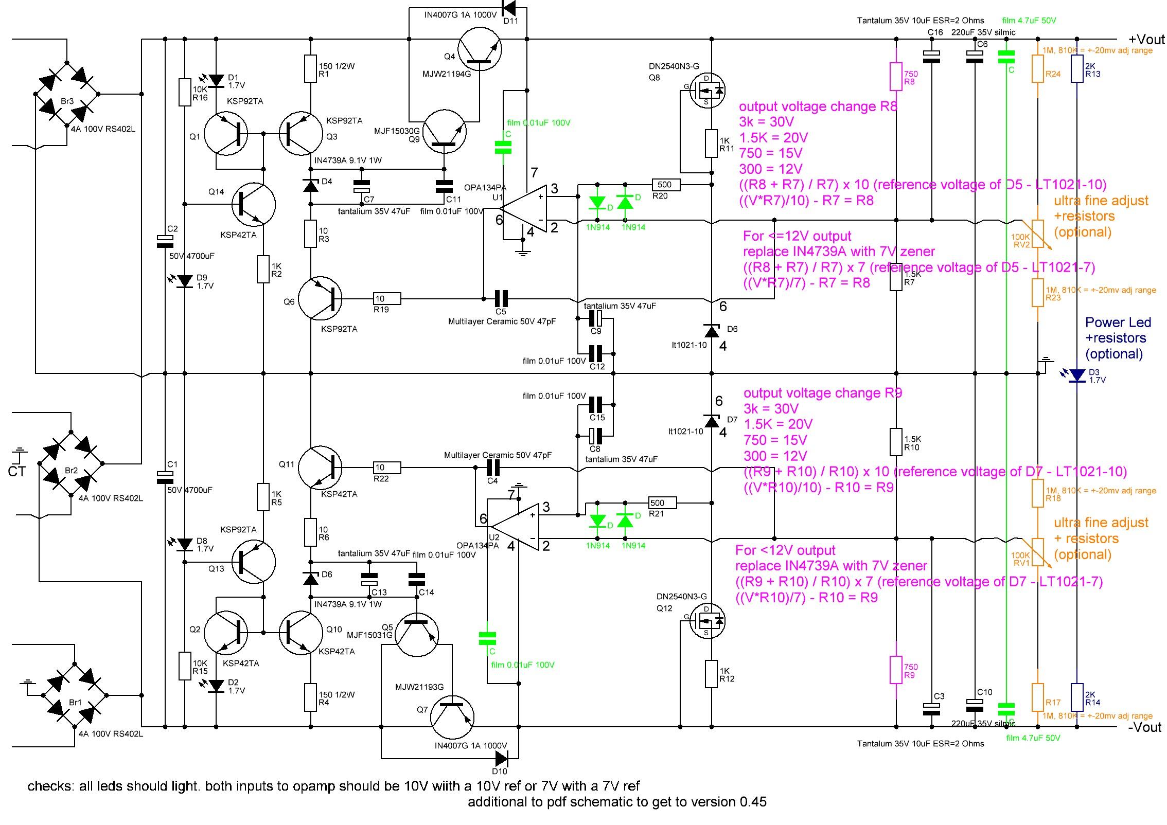
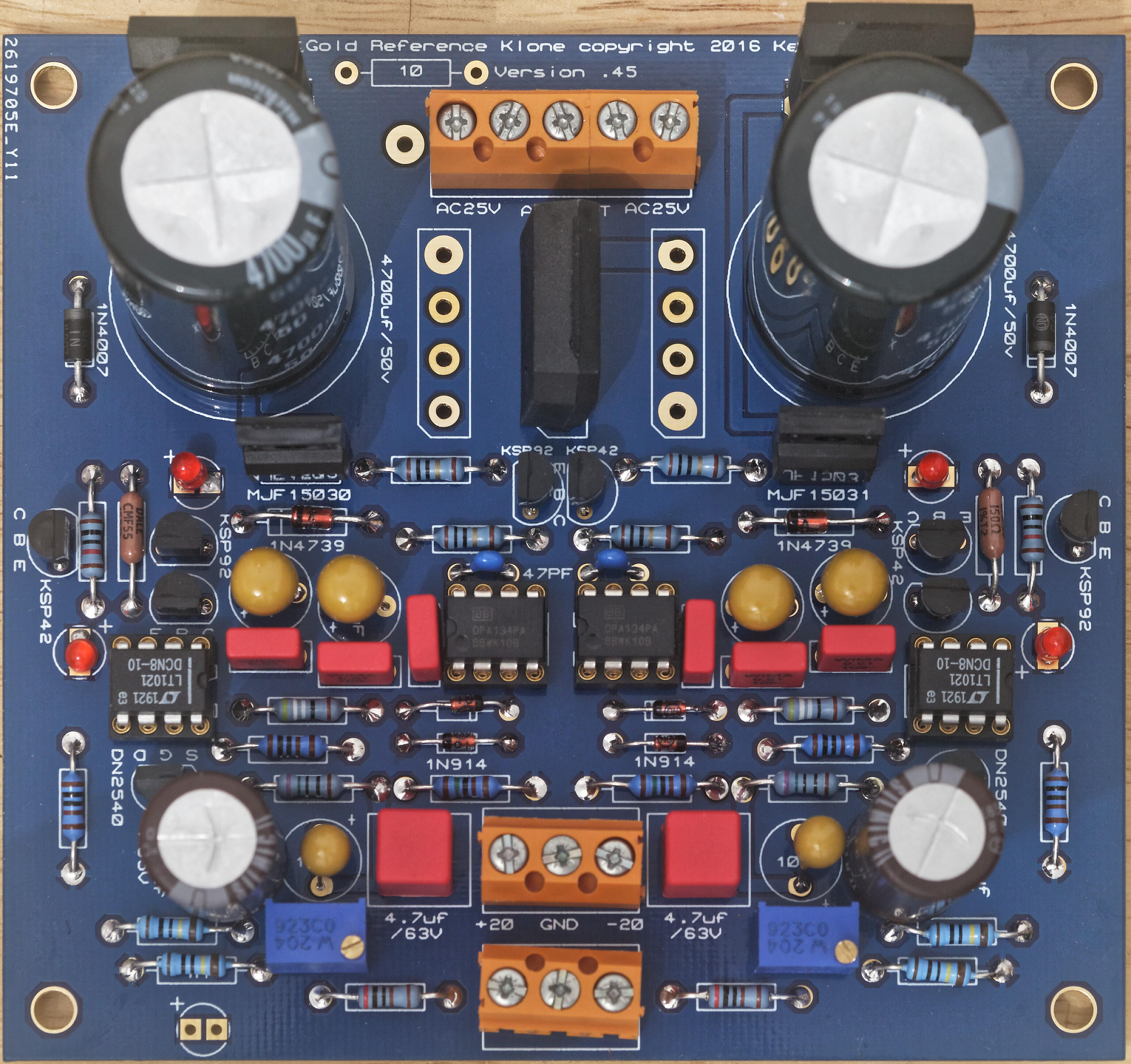
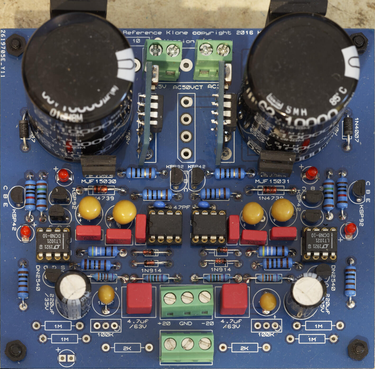
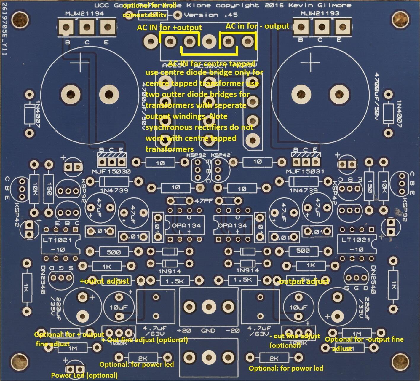
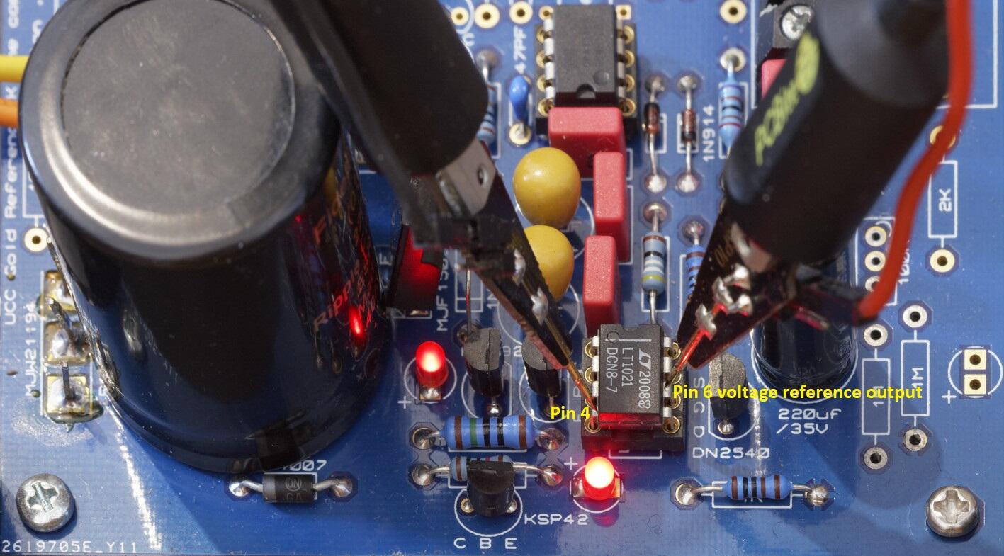
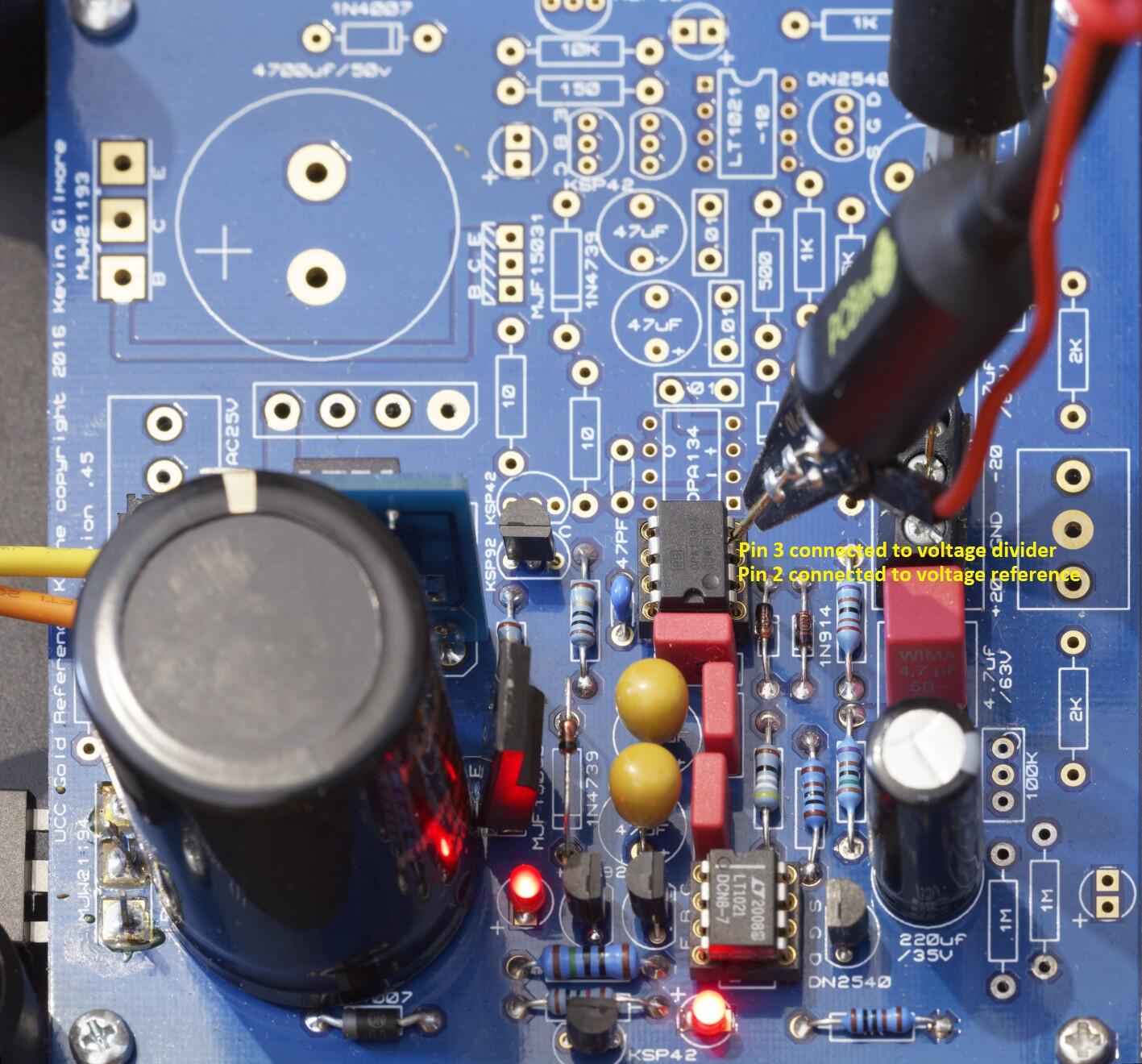
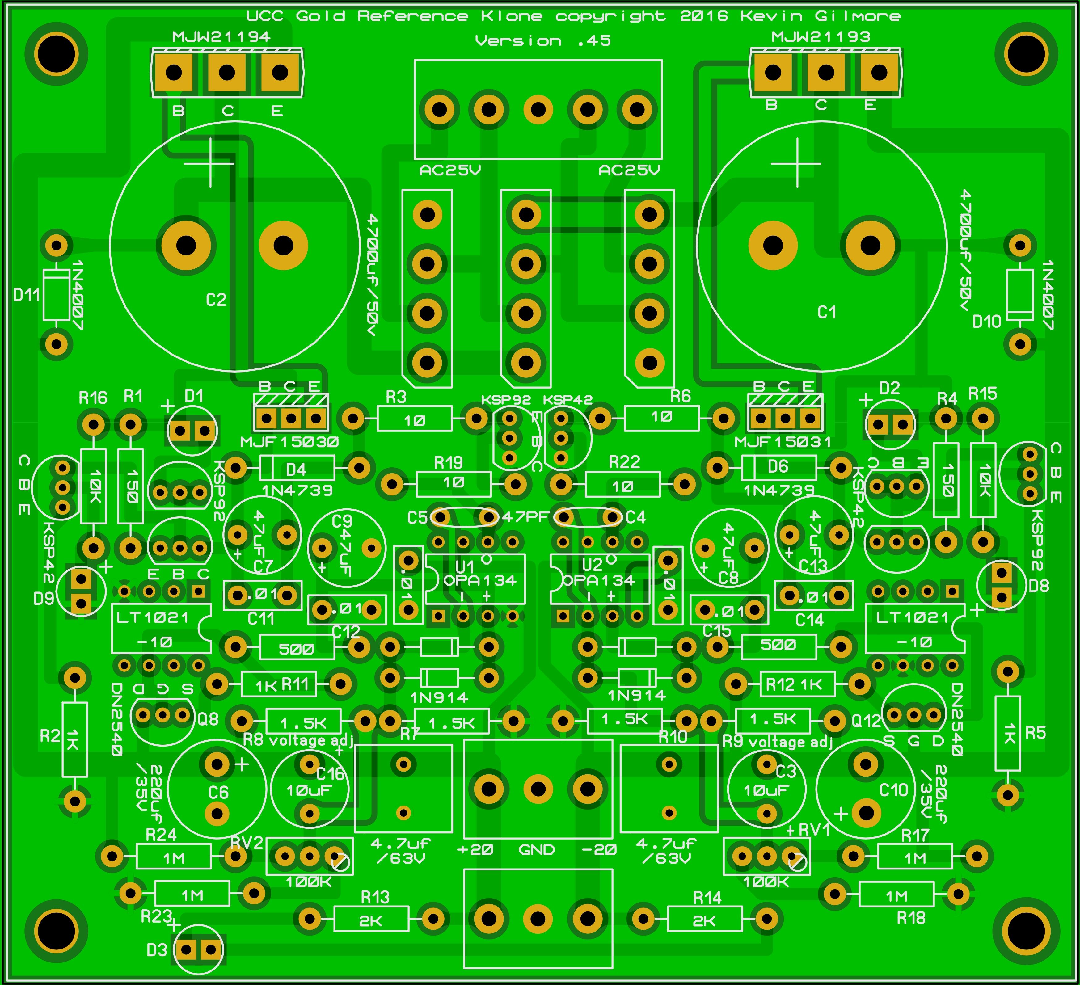
Golden Reference LV Build Guide Schematic for the golden reference LV: parts in green are new additions compared to the published schematic pdf in joamats post above. Parts in purple set the output voltage, parts in brown are the optional fine output adjust and parts in dark blue are the optional power led. Component Layout Optional parts and Options: 1. if you don't want to have a power led fed from the LV board omit the 2K resistors R13, R14 and the led D3 2. if you don't want very fine adjustment of the output voltage omit the 1M resistors R17, R18, R23, R24 and the trimmers RV2 and RV1. If you want more adjustment range reduce the value of the resistors. With 1M ohm resistors the fine adjust can only change the output voltage by a few mV. Replacing with 810K resistors provides a little more adjustment range ~ 20mV but at the expense of decreasing the temperature stability. A cheaper alternative for good output accuracy is to use 1/4W 0.1% low ppm e.g. 15ppm resistors for the voltage set resistors and omit the fine adjust completely - which is cheaper and improves the temperature stability. 3. if you have the dual output board (which has both positive and negative output rails) either you populate the middle diode bridge only and use a transformer which is centre tapped OR you populate the two outer diode bridges and use a transformer with two separate output windings. If use use synchronous rectifiers instead of diode bridges use must use the second option and use separate windings for positive and negative rails. Do not populate all three bridges. If you use a centre tapped transformer you must connect the centre tap to the middle screw terminal (which is connected to the GRLV ground plane) of the 5 terminal AC input block . Do not use a synchronous rectifier to the centre bridge it will not work correctly and can result in the driver mosfets of the synchronous rectifier burning. Note the GRLV cant output less than the voltage of the voltage reference (LT1021), ideally for proper regulation the output needs to be more than about 2V higher than the LT voltage reference. So for about 12V or less output it is recommended you change the 10V reference for a 7V and the zener diodes for a 7V. For 12V output 10V reference or 7V reference can be used but the 7V reference version may have less noise. Maximum output is constrained by the voltage rating of the caps and is about 30V without modifications. Setting the Output Voltage For the positive output R8 and R7 control the output voltage along with the voltage reference, the output voltage is ((R7+R8)/R7)*voltage reference output D5. Assuming you keep R7 at the stock value of 1.5K: output voltage change R8 to 3k = 30V 1.5K = 20V 750 = 15V 300 = 12V In general to calculate R8: ((Voltage required * R7)/voltage reference D5 output) - R7 = R8 For the negative output R10 and R9 control the output voltage along with the voltage reference, the output voltage is ((R10+R9)/R9)*voltage reference output D7. Assuming you keep R10 at the stock value of 1.5K: output voltage change R9 to 3k = 30V 1.5K = 20V 750 = 15V 300 = 12V In general to calculate R9: ((Voltage required * R10)/voltage reference D7 output) - R10 = R9 Photos of finished boards for reference: This version uses a single diode bridge so this is setup for a centre tapped transformer, also has the trimmers and resistors for the power led populated but no power led installed. The build uses 4700uF reservoir caps and silmic 220uf output caps and 1/4w resistors from vishay and dale. This is what you get using the BOM link in this post (see bellow) and is very close to the original BOM published near the beginning of this thread. This version is setup for dual separate transformer windings, and has no power led or trimmers implemented. It also uses synchronous rectifiers instead of diode bridges, nippon chemicon 10000uF reservoir caps, Panasonic FR series 220uF caps and 1/2W 50ppm 1% koa resistors. The resistors that set the output voltage are 1/4W TE 0.1% 15ppm for increased temperature stability and output accuracy. This is my current default build. BOM (based on 10V voltage reference and all options being populated) https://www.mouser.com/ProjectManager/ProjectDetail.aspx?AccessID=edda1bdbf7 Component list with cap size information Br1,Br2,Br3 = 2 x 4A 100V RS402L use 2 for dual winding transformer use 1 for centre tapped transformer C,C = 2 x film 4.7uF 50V 5mm lead spacing 0.5mm lead diameter C,C,C11,C12,C14,C15 = 6 x film 0.01uF 100V 5mm lead spacing max size ~ 7.6mmx3mm 0.5mm lead diameter C1,C2 = 2 x 50V 4700uF 10mm lead spacing max diameter 25mm, 22mm more comfortable fit main reservoir cap I also use Nippon Chemicon 63V 10000uF which just fit. C3,C16 = 2 x Tantalum 35V 10uF ESR=2 Ohms 5mm lead spacing 0.5mm lead diameter C4,C5 = 2 x Multilayer Ceramic 50V 47pF 5mm lead spacing 0.5mm lead diameter C6,C10 = 2 x 220uF 35V silmic or Panasonic FR series 5mm lead spacing 12.5mm max diameter C7,C8,C9,C13 = 4 x tantalium 35V 47uF ESR=0.8ohms 5mm lead spacing 0.5mm lead diameter D,D,D,D = 4 x 1N914 D1,D2,D3,D8,D9 = 5 x 1.7V red led 4 are required one is for optional power led leally all 4 main leds should be from the same batch and have similar characteristics. D10,D11 = 2 x IN4007G 1A 1000V D4,D6 = 2 x IN4739A 9.1V 1W use 7V zener for <=12V output D6,D7 = 2 x lt1021-10 10V voltage reference use 7V for <=12V output Q4 = 1 x MJW21194G Q5 = 1 x MJF15031G Q7 = 1 x MJW21193G Q9 = 1 x MJF15030G Q1,Q3,Q6,Q13 = 4 x KSP92TA Q2,Q10,Q11,Q14 = 4 x KSP42TA Q8,Q12 = 2 x DN2540N3-G R1,R4 = 2 x 150 1/2W R13,R14 = 2 x 2K R15,R16 = 2 x 10K R17,R18,R23,R24 = 4 x 1M, 810K = +-20mv adj range optional for fine adjustment R2,R5,R11,R12 = 4 x 1K R20,R21 = 2 x 500 R3,R6,R19,R22 = 4 x 10 R7,R10 = 2 x 1.5K R8,R9 = 2 x 750 for 15V output change as necessary for your output RV1,RV2 = 2 x 100K optional for fine adjustment U1,U2 = 2 x OPA134PA opamp Building Once you have decided the build options and output voltage, construction is straightforward given there are no high voltages. Depending upon the current draw the large power transistors on the side of the board may require heatsinking. The metal tab is live so they will need to be insulated from the heatsink/chassis. Socketing the reference and opamps is optional but it does make replacement and reuse easier. Make sure the caps are installed with the correct polarity. The line on the tantalums denotes the positive Terminal whereas the line on electrolytic caps denotes the negative terminal.... the film caps can be installed either way around as can the small ceramic caps. For the leds the longer leg is the + leg and this goes to the + mark on the pcb be careful to install the opamps and voltage reference chips the correct way around they will get very hot very quickly if installed the wrong way. make sure you don't place as ksp42 where a ksp92 should go of visa versa. Its easy to do since they look identical and its not easy to see all the markings once populating the board is finished. Testing (optional) If you have a means to control the input voltage to the board e.g. a variac, then with no load connected to the grlv the outer leds (closest to the LT voltage reference) should just start to glow at about 2.4 to 2.5VAC rms input voltage to the board and the output of the GRLV should be around 1V DC. If you cant get the outer leds to light with about 3VAC rms input, stop and disconnect, something is definitely wrong. By 3VAC rms the outer leds should be bright. Increasing the variac output further should see proportional rises in the GRLV DC output voltage until the output reaches the expected output. At this point the inner leds closest to the zener diode may not have lit and although basic regulation has been achieved, the input voltage is too low for full low noise regulation. Increase the input voltage a little more and the inner leds should light. This should happen with after about an additional 1 volt AC rms is added to the input. The output voltage should not increase. As a very rough rule of thumb, without load, the grlv needs about 2V less input AC rms than its DC output. So for example for 12v output expect regulation to just happen at about 10VAC rms input but the inner led not to light until about 11VAC rms. Note this figures depend on tolerances, the diode bridge voltage drop, led characteristics etc and are a rough guide only. Adding a load to the GRLV will mean it needs a higher input voltage in order to regulate since some of the sources of voltage drops are dependant on current draw e.g. the diode bridges. So if you adjust the variac to just get the inner led lit with no load don't be surprised if it goes out when you draw a few hundred milliamps. Another way to test is to connect the AC in of one rail to a current limited DC power supply. Set the current limit to say 0.010A (10mA) and slowly increase the voltage. Bellow about 3.3VDC input to the GRLV there should be low current draw <10mA. At about 3.4VDC the outer led will start to light and current draw should still be <10mA. Around 8.5VDC input current draw should reach about 10mA. The inner led close to the main cap should begin to light at about 2.6VDC input above the expected output e.g. 14.6VDC input for 12V output. At this point current draw should be about 20mA and you may need to increase your DC power supply current limit. Increasing the DC power supply output past this point should not result in increasing current draw or increasing GRLV output. Note when you increase the DC power supply voltage you will get an initial current draw spike as the input cap charges to the new voltage level but the current draw should quickly subside to the figures shown. If the GRLv regulates and behaves as expected with no load and has no warm components or varying output then you could continue to load testing. The reality is that if your RLV works with no load its almost certainly ok and will be fine without load testing. But if you want to be extra careful the easiest way to do this is with an electronic DC load. I setup my load so that it will abort the test if the output voltage of the GRLV exceeds 0.2V above or bellow the no load output. A properly working GRLV with enough input voltage will vary very very little with current draw - much less than a traditional 78xx/79xx voltage regulator. I then load at 50mA and check for hot components, and then in 100mA steps up to 1A. Above about 400mA the large main transistors will get hot if they are not heatsinked... this is normal as the current draw increases there is more power dissipation in the transistor. Note transformers and diode bridges etc do drop more voltage as the current draw increases so if the inner led goes out at higher current draws check the input voltage to the GRLV has not decreased too much for the GRLV to regulate. Don't load test about above 300mA for long periods without heatsinking the main transistors. Additional Checks (useful if troubleshooting) The voltage reference output voltage should be present between pins 4 and 6 of the LT reference and be stable and very close to the spec sheet voltage. Use fine tip probes and be careful not to short any pins together when probing: The opamp compares the voltage reference with the output voltage from the voltage divider (the resistors which set the output voltage) and creates a correction signal. Pin 2 of the opamp is connected to the voltage reference and pin 3 is connected to the voltage divider. When working correctly, the voltages with respect to ground to pin 2 and from ground to pin 3 should be identical and be the same as the output of the voltage reference measured above. In circuit testing and troubleshooting So its not working correctly or you want to do some more tests before powering on for the first time?. Here are some tests you can do on a fully built GRLV that has no power connected. With a multimeter set to diode check mode and the caps on the grlv fully discharged. you can do some sanity checks. The exact measurements will vary from multimeter to multimeter and device to device but this should give some ball park figures. My figures are based on a Brymen bm869s. Led polarity outer leds closest to the edge of the pcb and the voltage reference: red lead of multimeter to + lead of led, black on - lead of led ~ 0.8V slowly rising as a cap charges led does not light. leads reversed: 1.63V slowly rising led does not light inner leds closest to the main input filter caps: red lead of multimeter to + lead of led, black on - lead of led ~ 1.7V stable voltage led should light. leads reversed: over range / OL / open circuit, led does not light. Zener check both zeners close to the inner leds: red probe on band side black on non band side: OL / open circuit, probes reversed 0.66V Transistor Death/Incorrect Placement Checks large MJW21194 on +rail measuring looking at the front of the transistor where the markings are: red probe on left pin black on middle pin: 0.46V steady, probes reversed OL / open circuit red probe on left pin black on right pin: 0.48V steady, probes reversed OL / open circuit red probe on middle pin black on right pin: 0.5V rising rapidly, probes reversed 0.48V rising much more slowly large MJW21193 on -rail measuring looking at the front of the transistor where the markings are: red probe on left pin black on middle pin: OL / open circuit , probes reversed 0.48V steady red probe on left pin black on right pin: OL / open circuit, probes reversed 0.49V steady red probe on middle pin black on right pin: 0.48 rising slowly, probes reversed 0.5V rising much more rapidly MJW15030 on +rail next to inner led: red probe on left pin black on middle pin: 0.57V steady, probes reversed OL / open circuit red probe on left pin black on right pin: 0.57V steady, probes reversed OL / open circuit red probe on middle pin black on right pin: OL / open circuit , probes reversed 0.46 steady MJW15031 on -rail next to inner led: red probe on left pin black on middle pin: OL / open circuit, probes reversed 0.57V steady red probe on left pin black on right pin: OL / open circuit probes reversed 0.57V steady red probe on middle pin black on right pin: 0.48 steady probes reversed OL / open circuit KSP42 on +rail on edge of board: looking at flat front where the marking are red probe on left pin black on middle pin: 1.8V rising, probes reversed 0.6V steady red probe on left pin black on right pin: 1.2V rising, probes reversed OL / open circuit red probe on middle pin black on right pin: 0.6V steady probes reversed OL / open circuit KSP92 on -rail on edge of board: looking at flat front where the marking are red probe on left pin black on middle pin: 0.61V steady, probes reversed 1.7V rising red probe on left pin black on right pin: OL / open circuit. probes reversed 0.9V rising red probe on middle pin black on right pin: OL / open circuit, probes reversed 0.6V steady DN2540 on +rail between voltage reference and 220uf output cap red probe on left pin black on middle pin: 0.31V steady, probes reversed 0.32V steady red probe on left pin black on right pin: 0.004V steady. probes reversed 0.004V steady red probe on middle pin black on right pin: 0.32V steady, probes reversed 0.32V steady DN2540 on -rail between voltage reference and 220uf output cap red probe on left pin black on middle pin: 0.32V steady, probes reversed 0.32V steady red probe on left pin black on right pin: 0.004V steady. probes reversed 0.004V steady red probe on middle pin black on right pin: 0.32V steady, probes reversed 0.32V steady KSP92 on +rail near centre of board close to middle diode bridge: looking at flat front where the marking are red probe on left pin black on middle pin: 0.6V steady probes reversed OL / open circuit red probe on left pin black on right pin: 1.0V rising slowly, probes reversed OL / Open circuit red probe on middle pin black on right pin: rises to about 0.67V, probes reversed 0.56 steady KSP42 on -rail near centre of board close to middle diode bridge: looking at flat front where the marking are red probe on left pin black on middle pin: OL / Open circuit, probes reversed 1.61V steady red probe on left pin black on right pin: OL / open circuit. probes reversed 0.95V rising red probe on middle pin black on right pin: 0.59V steady, probes reversed 0.67V steady the pair of KSP92 on +rail ksp92 closest to voltage ref: looking at flat front where the marking are red probe on left pin black on middle pin: 0.62V steady probes reversed OL / open circuit red probe on left pin black on right pin: OL / open circuit, probes reversed 0.61 steady red probe on middle pin black on right pin: OL open circuit, probes reversed 0.61 steady the pair of KSP92 on +rail ksp92 closest to the inner led: looking at flat front where the marking are red probe on left pin black on middle pin: 0.59V steady probes reversed OL / open circuit red probe on left pin black on right pin: 0.59V steady, probes reversed OL / open circuit red probe on middle pin black on right pin: 0V / short, probes 0V / short the pair of KSP42 on -rail ksp42 closest to voltage ref: looking at flat front where the marking are red probe on left pin black on middle pin: OL / open circuit, probes reversed 0.59V steady red probe on left pin black on right pin: OL / open circuit , probes reversed 0.59V steady red probe on middle pin black on right pin: 0V / short, probes 0V / short the pair of KSP92 on +rail ksp92 closest to the inner led: looking at flat front where the marking are red probe on left pin black on middle pin: OL / open circuit, probes reversed 0.61 steady red probe on left pin black on right pin: 0.62V steady probes reversed OL / open circuit red probe on middle pin black on right pin: 0.61V steady, probes reversed OL open circuit Good luck with your build and thank you to everyone who contributed to the design of the GRLV and this thread.
- 813 replies
-
- 19
-

-

-
Megatron Electrostatic Headphone Amplifier
jamesmking replied to kevin gilmore's topic in Do It Yourself
I truly feel sorry for you. I feel its totally unfair that someone should take the designs here and butcher them and then offer no actually useful support or help. At the very least they should supply proper electronic schematics for the power supplies and amp boards. That would help in debugging and finding out what is actually going wrong (probably multiple implementation issues). I see nothing here that remotely resembles a megatron build from the gerbers released on these forums. The golden reference HV is a low noise will respected power supply use in many amps here. Why did the creator of this amp not use it? this amp looks like its had lots of changes for changes sake rather than for any good reason. -
hi johnwmclean,
I have 4 spare ksc5026mos purchased from mouser in the USA - same batch as I am using in my T2 power supplies. I'm based in the UK. Swap wise the things I am short of are C2M1000170D, 2sk216 and 2sj79 - but I guess almost everyone is short of them.
regards
James
-
your dn2540 looks to be in backwards compared to the silkscreen.... the hashed section on the silkscreen indicates the metal tab... perhaps this could be because your silkscreen is wrong or maybe the builder has modified the pcb?? have you checked which pin is connected to what compared to the schematic? and looked at the dn2540 data sheet to confirm the orientation?
-
-
-
el84? - the spec sheets says thats 0.76A per valve for the heater.... http://www.r-type.org/exhib/aaa0028.htm T2 and most of kevins designs are EL34. EL34 is around 1.5A to 1.6A heater per valve. http://www.r-type.org/exhib/abv0058.htm As craig says its around 3A for a pair and separate heater windings for each channel... I use transformer windings rated at 4.5A and the extra 1.5A is simply a safety margin. Heater current draw will be higher when the heaters are cold (less resistance) but the current draw will decrease within a minute or as the heaters heat up and reach steady state. I aim for 50% margin on the transformer heater windings. I like to run the el34 heaters at 6V rather than 6.3 for longer life.
-
personally I use cal test silicon test lead wire. Its cat IV rated at 1KV , very flexible and can withstand 180C. Its also just copper strands with no plating. (I find almost anything silver plated to be bright sounding and have banned anything silver or silver plated from hifi). I also arrange the wiring to the plugs and sockets so that + voltages go in the top half, grounds and zero volts in a line through the middle and - voltages in the bottom half. This keeps the potential difference between any two pins to a minimum. when possible I leave unused pins around any especially high voltages. I also test with a insulation tester. At 1000V the insulation resistance must be off the scale and there must be >50Gohms resistance at 2500V between all adjacent wires. https://www.uni-trend.com/html/product/tyyq/Electrical/UT510_Series/UT513A.html