

Leaderboard
-
dsavitsk
High Rollers19Points4957Posts -
Augsburger
High Rollers16Points13165Posts -
Voltron
High Rollers12Points34563Posts -
blessingx
High Rollers11Points17710Posts




Popular Content
Showing content with the highest reputation on 11/18/20 in Posts
-
4 points
-
You never know when and where you will find the meaning of life It be here y'all3 points
-
3 pointsSince photography is a hobby of mine as well, I decided to take some internal and external pictures of my recently completed KGSSHV. Hope you enjoy them. Please click or copy/paste the Dropbox link below to view those pictures: https://www.dropbox.com/sh/4ox0xh7s1aiw5cb/AACdu5DpeRyeFuINloC8HkRFa?dl=03 points
-
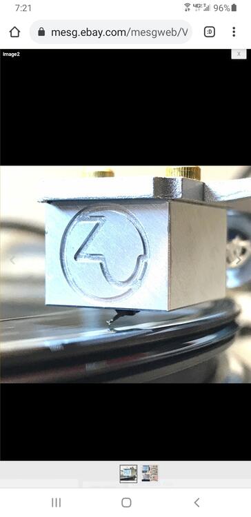
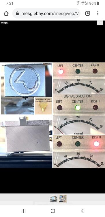
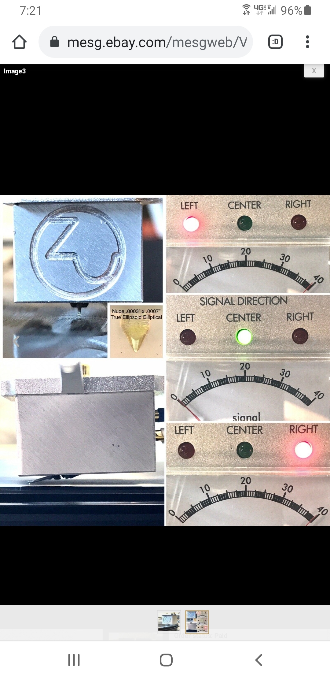
2 pointsThat's the problem, all the photos got nuked. It hasn't been shipped just yet, but it looks like the re-tipped Zu DL-103 tests out pretty darn good. He said that it's pretty rare to get separation so close to a perfect 40 degrees.
 2 points
 -
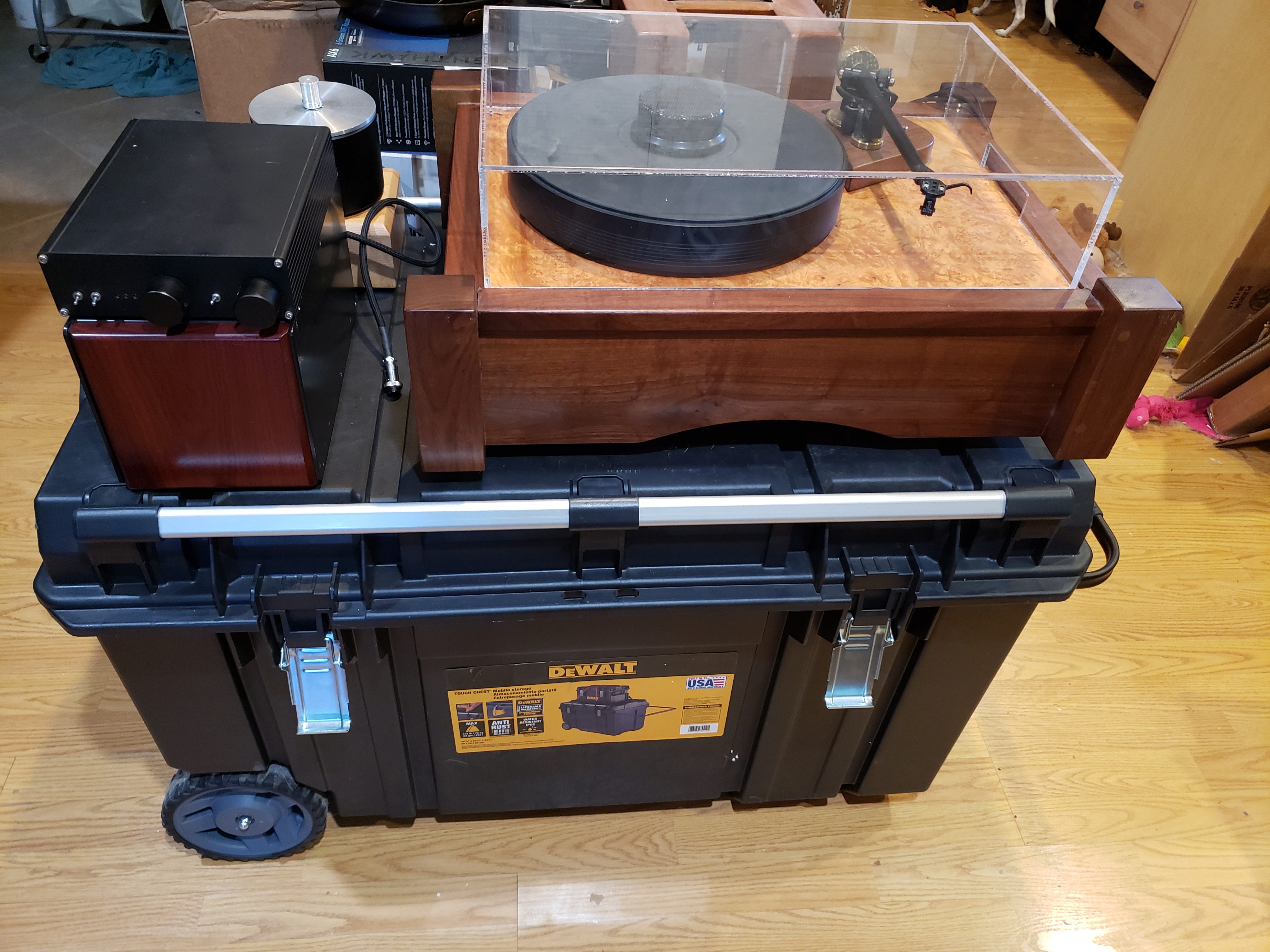
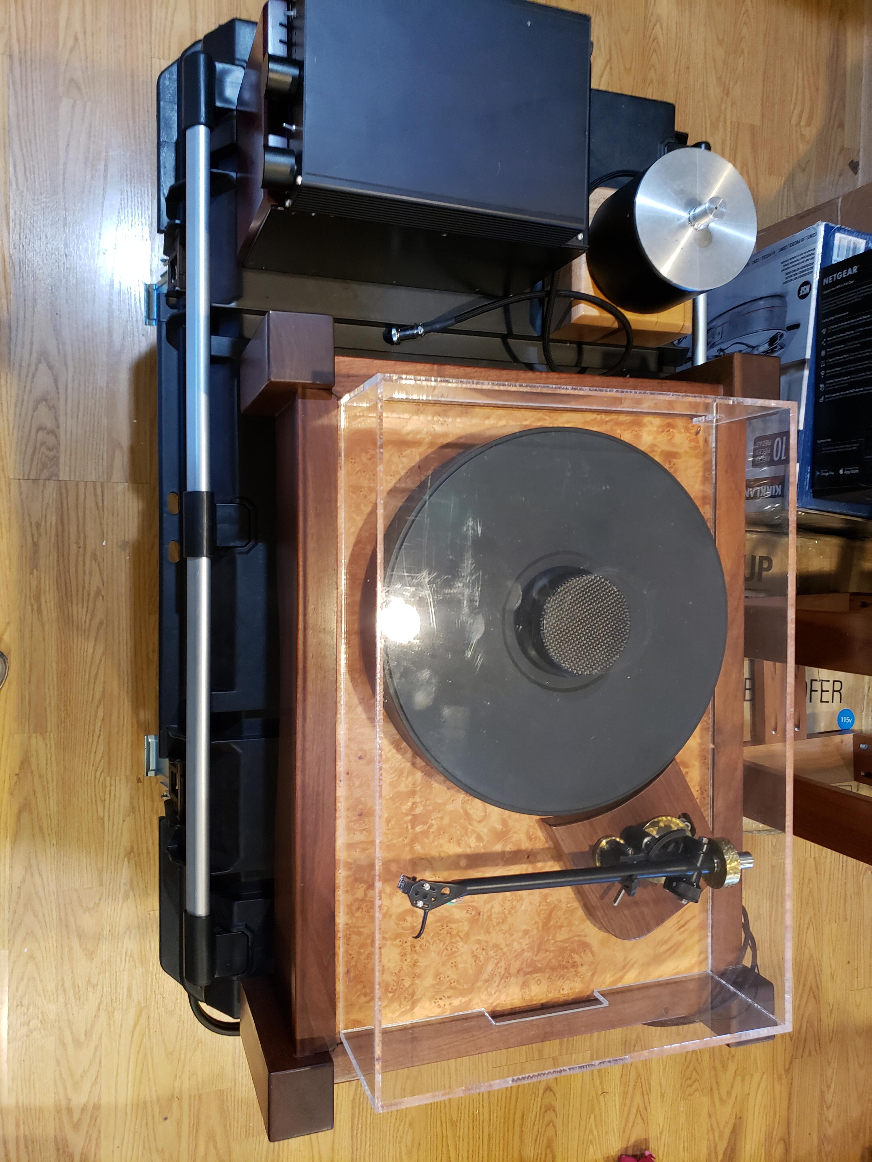
2 points2 pointsHeh. You got me! I officially put in to have 12/10 and 12/11 off. Don't screw me on this, CD Projekt!2 points2 pointsFrom my experience with my departed HE 4XX, they need it. Much prefer my modded T50RPs (Mk I). If you need to EQ phones, my thought has always been you have the wrong phones...2 points1 point1 pointHaven't I mentioned before that I'm just here to look pretty? I'll leave the technical mumbo-jumbo to the smarter people. 🙂1 point1 pointSo funny thing, barely related to video games. When CDPR announced they were delaying Cyberpunk yet again, their stock dropped. It's obviously going to go up. I called my broker (yes, I have one) and explained the situation. He knows fuck-all about video games, but he understood what I was talking about. I said "put be down for X shares!" He said sure. I got call back from him an hour later. Apparently it's impossible for Edward Jones (the firm I use) to buy CDPR stocks, for reasons that are unclear to me. Also I caused a mini drama in the east coast EdJo offices as calls went up and down the power structure as different suits and ties tried to figure out why CDPR is completely restricted from purchase. I think it has something to do with the Polish government.1 point1 pointBe careful, if his doesn't arrive by morning he will hijack one of the black helicopters fly to your house and steal yours.1 point1 point1 point1 point1 point1 pointWhy's that? EQing—whether through hardware or software—is relatively simple. It seems to provide a way to modify the frequency response of headphones that are technically competent but sonically unbalanced. For example, I like many of the attributes of the Koss ESP/95X, but they certainly benefit from a bit of EQ (in my opinion). And I don't use EQ on my Utopias, but that would seem to be a possible solution for many HCers that want to tame their treble and boost the bass a bit.1 point1 pointAgreed. Fantastic mini-series. Hawke's performance had light & shade I'd never seen from him before. That scene of Brown & Onion in the jail cell: “Whatever you are, Onion, be it in full. You were made by your maker, and he loves you. And I love you, too. I don’t care what clothes you wear any more than I do the size of your shoes.” "The Good Lord Bird doesn't fly in a flock. The voice of our spirit is gentle. Sometimes you have to fly alone to hear it" Whew!!!1 point1 pointNot entirely from scratch. I had a thread dedicated to the build, but it got nuked by Reks. I purchased a VPI Aries special edition Black acrylic platter, about 2" thick, along with the accompanying inverted platter bearing. Then purchased a Rega RB300 tonearm with upgraded Cardas wiring. Then outfitted that tonearm with Pete Riggle's counter weight and VTA mechanism. The plinth I built was rather complex, with 6 alternating layers of 3/4" birch plywood and 3/4" MDF. I drilled a series of 10 holes about 1 1/2" in diameter and 3" deep, on the bottom of the plinth. Those I filled with the modern version of lead shot, for even more anti resonate properties, and made removable caps, so that I could adjust fill levels accordingly. I wrapped the plinth core with 3/4" Walnut, Walnut corner posts and Big leaf Maple burl veneer on top. I made the tonearm board out of Walnut, and made it adjustable by about 1/2". Marc built me a Pass Pearl phono stage and also a DIY motor controller, for the separate motor pod and Maxon motor. The turntable weighs in at around 75 lbs. And it's enormous! Hence the name Colossus.1 pointVia: https://ftw.usatoday.com/2020/11/coca-cola-christmas-taika-waititi1 point1 point1 pointI finished Horizon Zero Dawn over the weekend on PC. Very cool game! The story was surprisingly good and a really cool take on what would otherwise be a familiar post-apocalypse trope. I mentioned to a buddy that maybe the reason there are so few great Sci-fi tv series these days is the games industry has picked off so much of the good writing talent? Also, it is a credit to how good the story is and how fun hunting robot dinosaurs is that the bad parts of the game (side quests, in-game economy, boring open world activities) really don't distract from the high points. The game is also really stunning in true 4k on PC.
.thumb.jpg.1b30faf1e7d6659828b111000d9195c5.jpg)
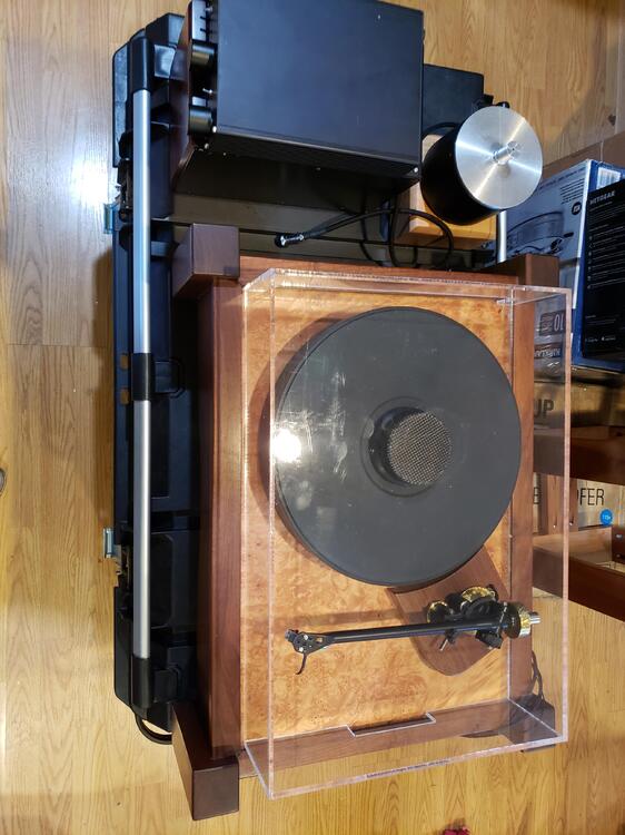
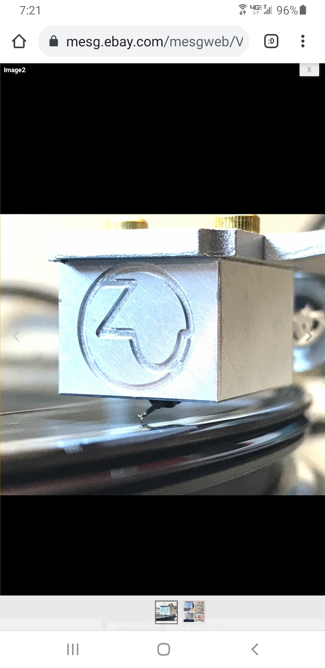
.thumb.jpg.6a68a973d8995a55ef6eea96cbab25a9.jpg) 1 point1 pointIT'S BACK! I remember it being big, but I forgot how massive it is. In no way is it going to fit on the TT stand I just built. I've also forgotten the layout of the controls on the speed controller, and which is input and output on the DIY Pass Pearl phono stage. Lots of fiddling to do before I'm near ready to fire up the beast, but it feels good to have her home again. It was 12 years ago that I built her. I need to see if I can get the Zu Audio DL 103 aluminum bodied cartridge repaired. I had broken the cantilever some years back. I also need to source a rubber belt for the motor/platter. Damn this thing is big!
1 point1 pointIT'S BACK! I remember it being big, but I forgot how massive it is. In no way is it going to fit on the TT stand I just built. I've also forgotten the layout of the controls on the speed controller, and which is input and output on the DIY Pass Pearl phono stage. Lots of fiddling to do before I'm near ready to fire up the beast, but it feels good to have her home again. It was 12 years ago that I built her. I need to see if I can get the Zu Audio DL 103 aluminum bodied cartridge repaired. I had broken the cantilever some years back. I also need to source a rubber belt for the motor/platter. Damn this thing is big!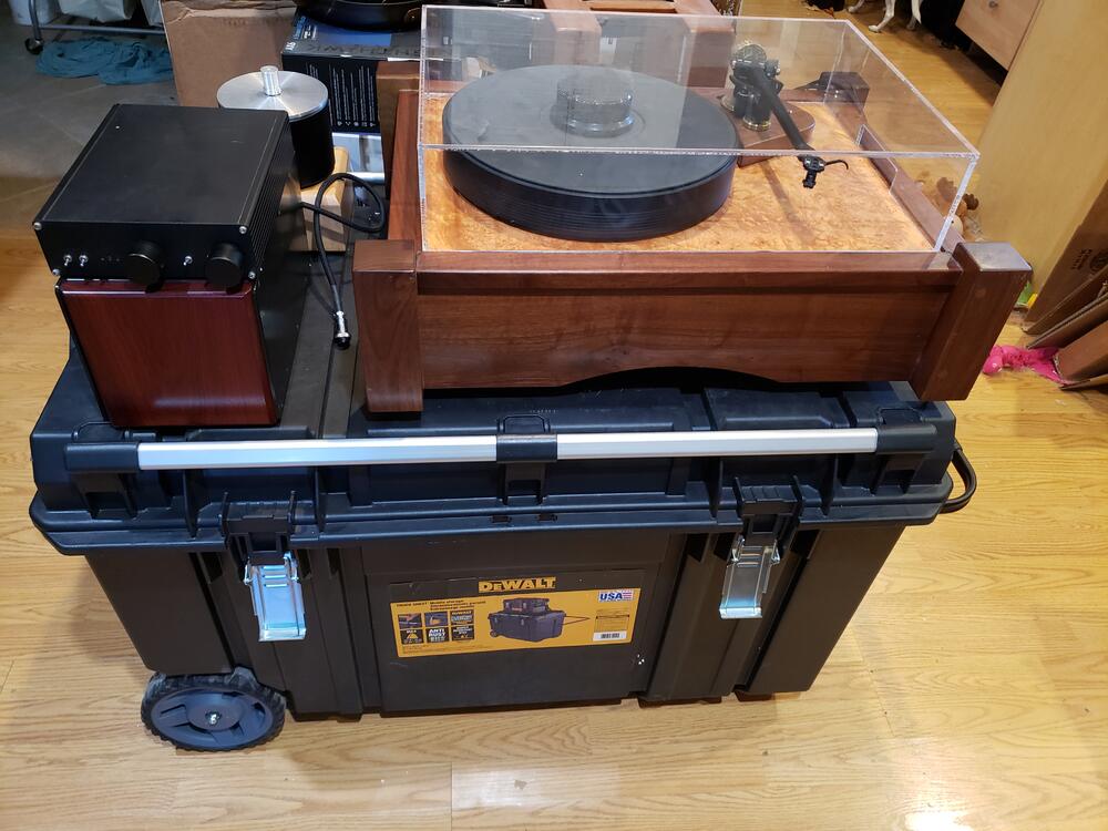
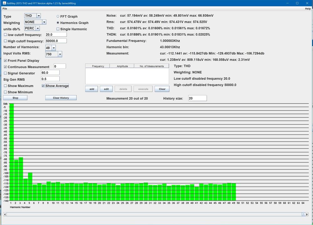
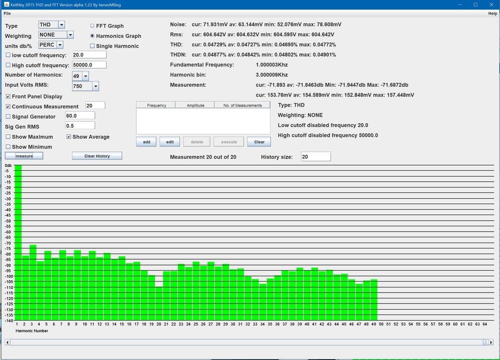
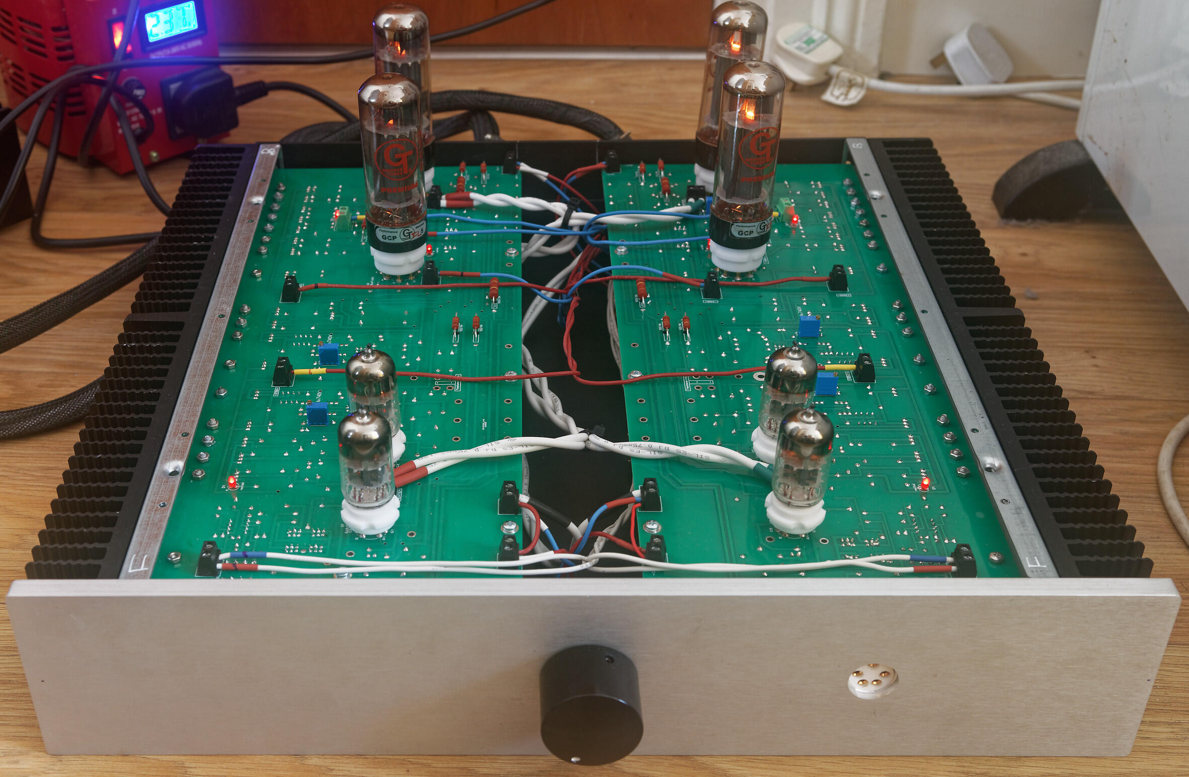
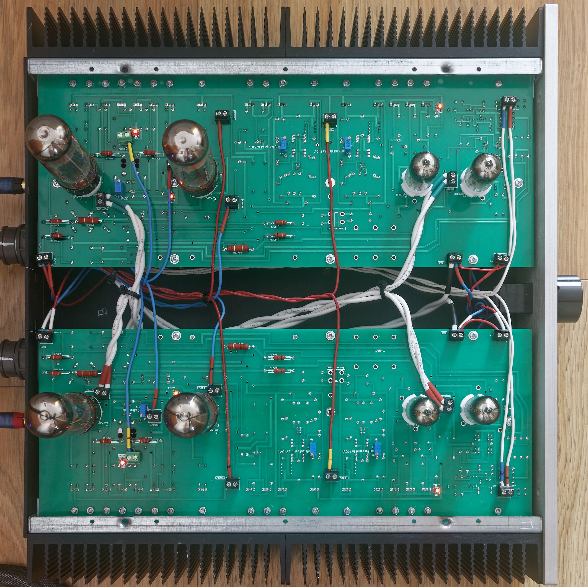
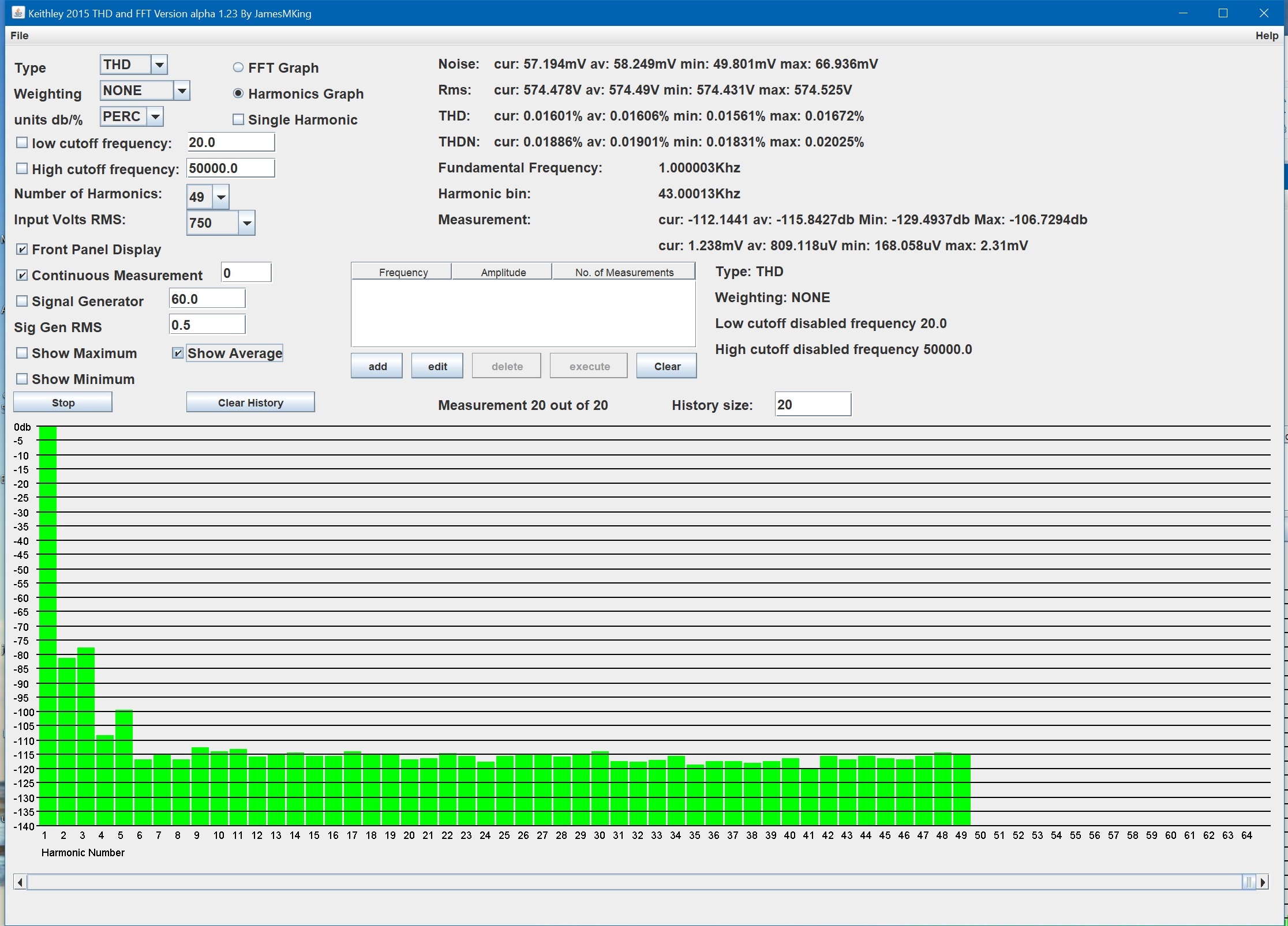
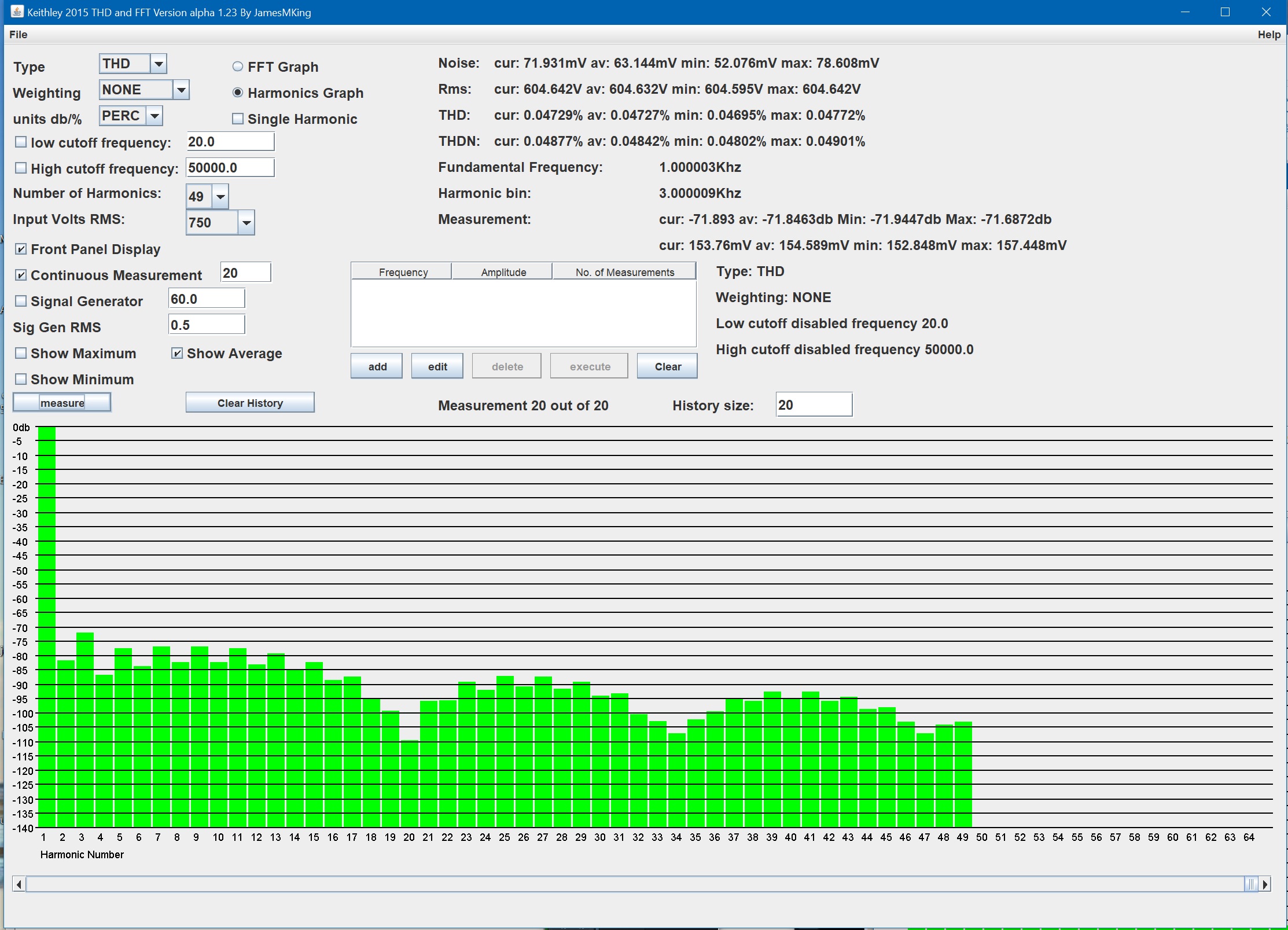
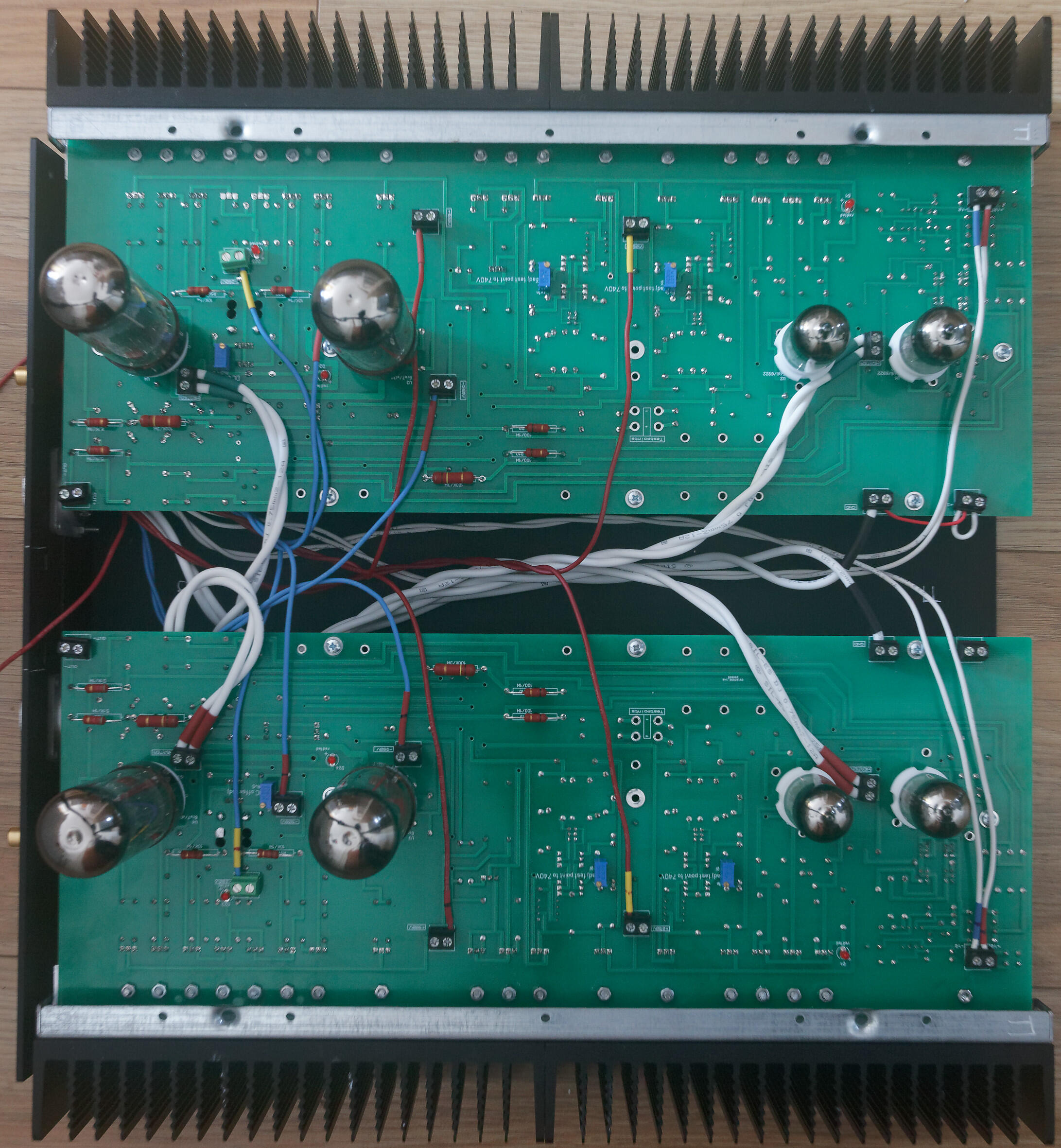
 1 point1 pointlisten to it? if you check my todo list nowhere does it say listen to it... measure it yes... listen to it? why would I do that? 🙃 latest update, internal signal wiring done (silicone not cardas - I need to buy more cardas chassis wire) and front panel completed. Both channels powered up at the same time for the first time. No drama so far. The heatsinks around the el34s runs a bit hotter than joamats mini T2. I not done any temperature checks look good. All transistors seem ok and so do the high power resistors. .6922 heater voltage is a little high at 6.35V so I will need to add some dropper resistors. All other voltages are spot on. El34 heaters are at 6.1V which is about the same level as my mini T2. I found my first issue, the DC balance between + and - halves of a channel is fine <50mv BUT the DC offset to ground started at -85V and even adjusting the offset pot all the way I only got it down to -33V. Exactly the same on the other channel due to close matching of components and matched valves. So I will need to replace the dc offset adjustment trimmers with something 2-3x the range. Anyway I know you have been waiting for the money shot: glowing leds and heaters so enjoy: Im currently going for an extended power on idle test and will be periodically checking voltages and temperatures on both the amp board and psu. If that passes it will be time to feed it some test signals... I hoping for more detail in the square waves, more dynamics in the triangle waves and smooth fatigue free sine waves. Here are the first measurements. Distortion 1Khz input Total Harmonic Distortion to 49Khz is around 0.0063% unweighted (average of 20 measurements) 2nd harmonic is around -90db and third slightly higher at -87db. The other harmonics are very low all less than -105db. total harmonic distortion plus noise is better than 0.018% (im not using shielded cables for this test AND the amp and psu do not have top lids and the cases are not grounded so the amplifier is almost certainly has better thd+n than I am measuring in this setup. At around 575V rms 5th harmonic starts to rise and at 600Vrms output all harmonis increase and odd order are higher than even order harmonics. NOTE this measurements where taken with around 35V DC offset so it is possible clipping may occur a little later with less offset... Noise, THD, THD+N and level of distortion harmonics at 575V RMS, 1Khz output: Noise, THD, THD+N and level of distortion harmonics at 600V RMS output 1Khz: The THD up to 49Khz is still less than 0.05% The amp runs quite a bit hotter than the mini T2, heatsinks near the EL34s run at 40C and power consumption is close to 205W. The mini T2 is around 153W. The power supply is also is less efficient than the golden reference HV, the 3W resistors between the ksa1156es and ksc5026 run close to 90C and dont have a lot of room around them, on one side there is a large 0.1uF 1KV film cap and on the other 5 closely packed transistors... So the T2 needs good heat sinking and the psu boards could do with lengthening a little to give the 3W resistors a little more air flow around them and drill holes under them. Update DC offset fix, The 5K pot in parallel with the 510 ohm emitter resistor gives a minimum resistance of about 461ohm which still gaves me ~ -33V offset. With the 5K pot in the middle you get around 423ohm combined resistance and ~ -85V offset. So I replaced the 510ohm with 604ohm and this gives enough adjustment range to get <1V DC offset. (I would have implemented joamats suggestion but I did not have any 10K pots)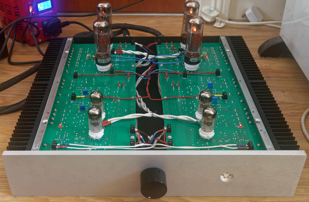
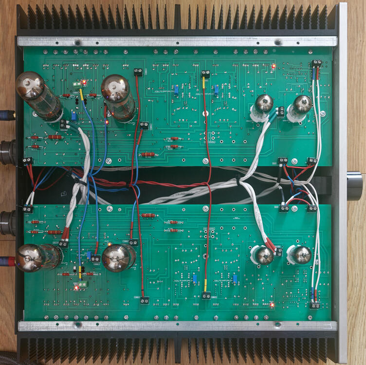
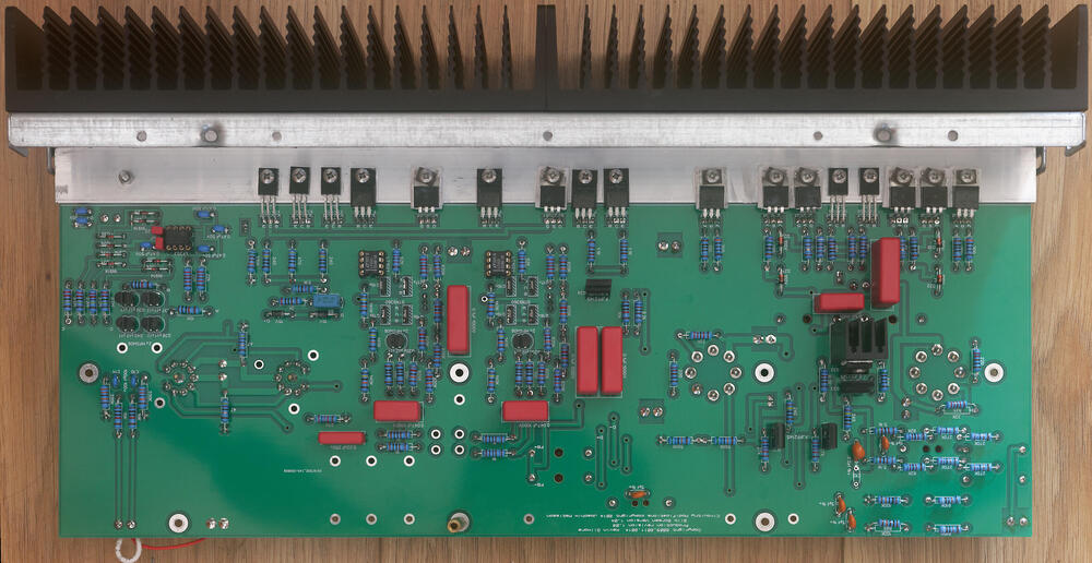
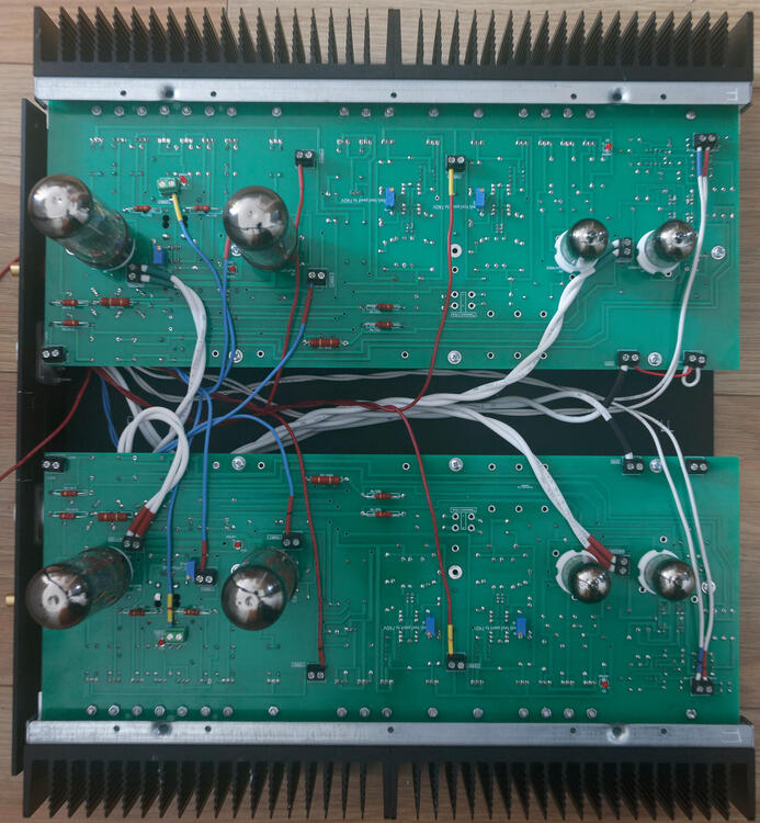
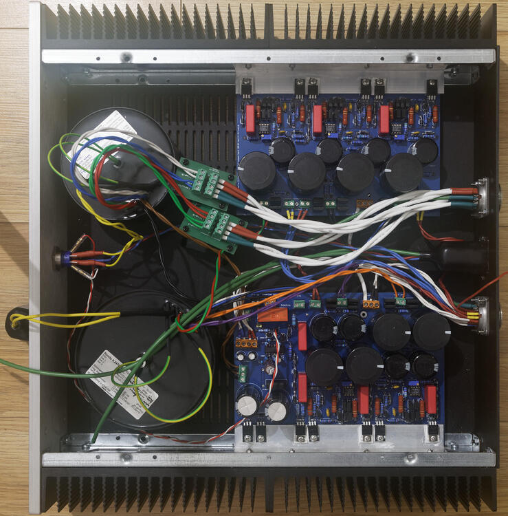
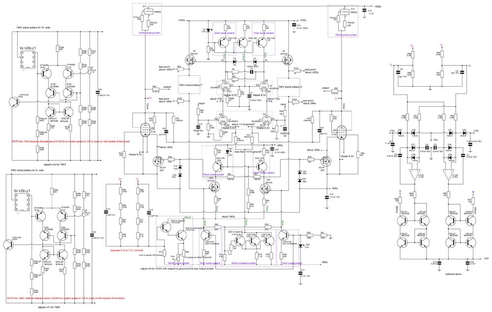
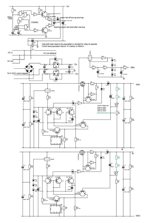
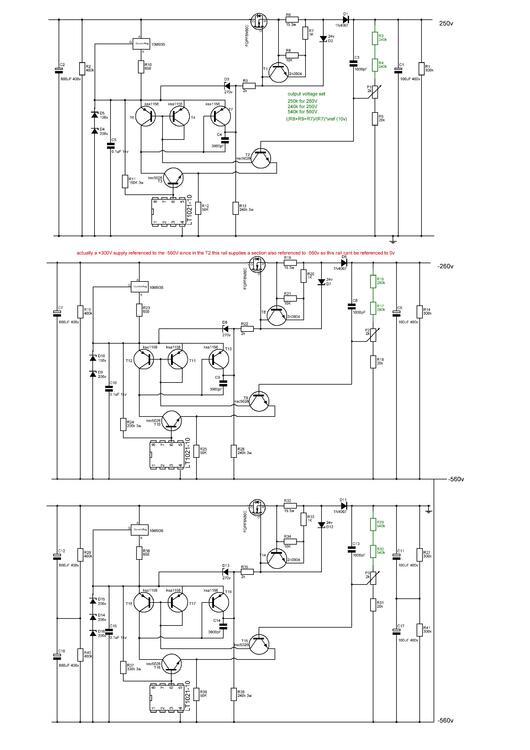
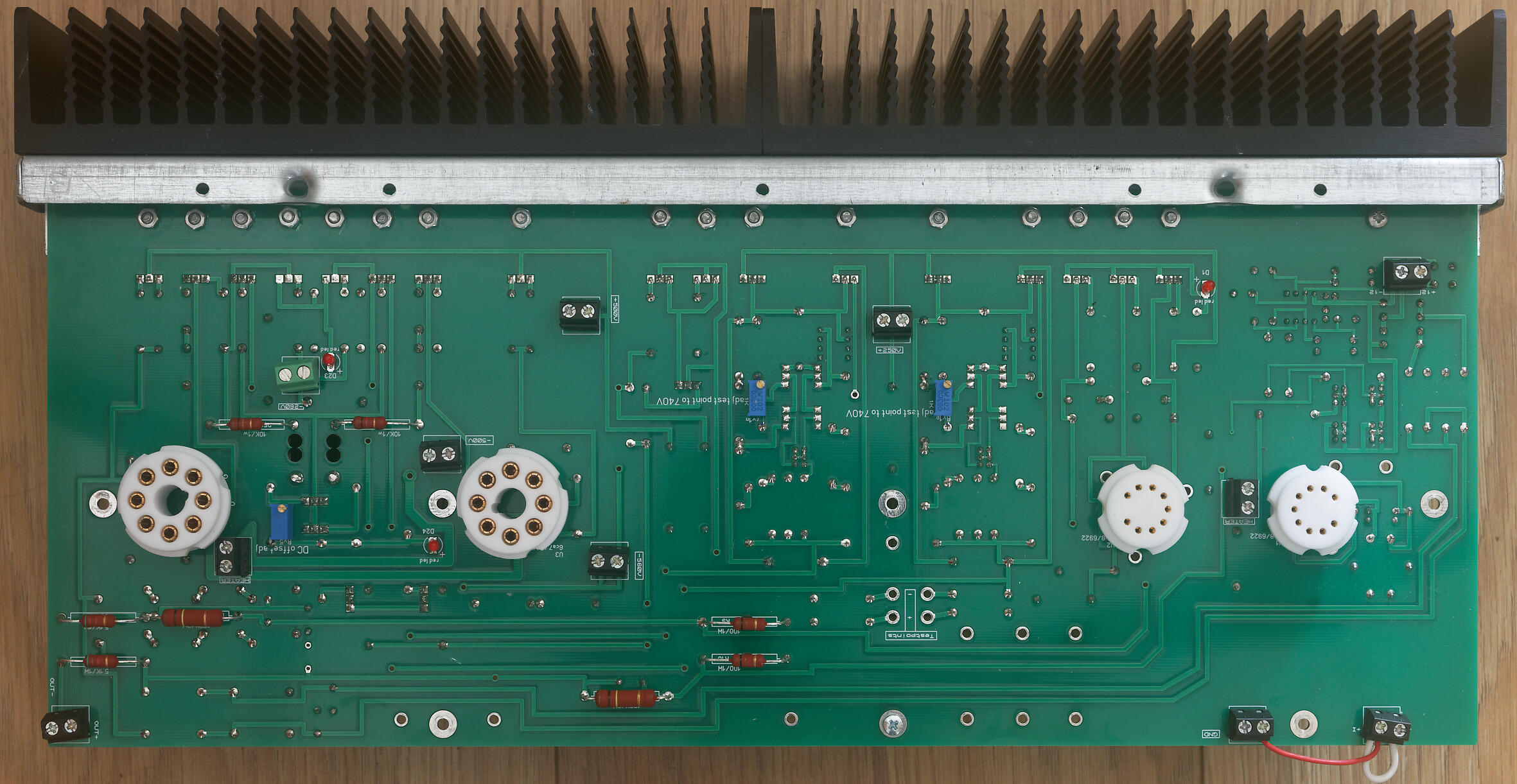
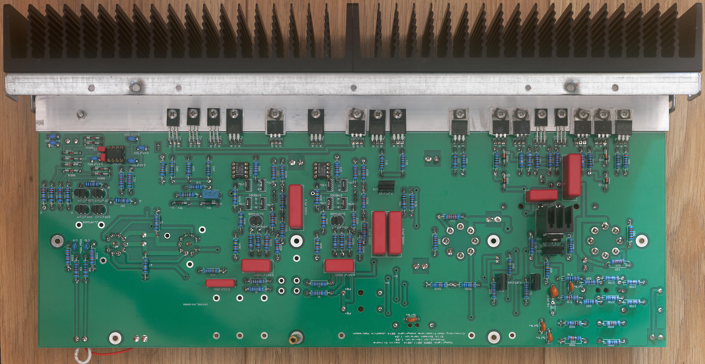
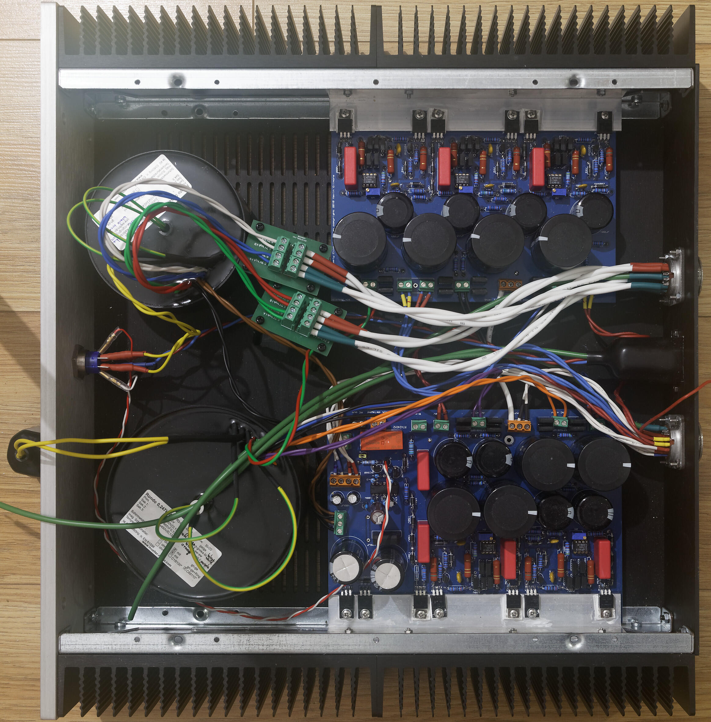
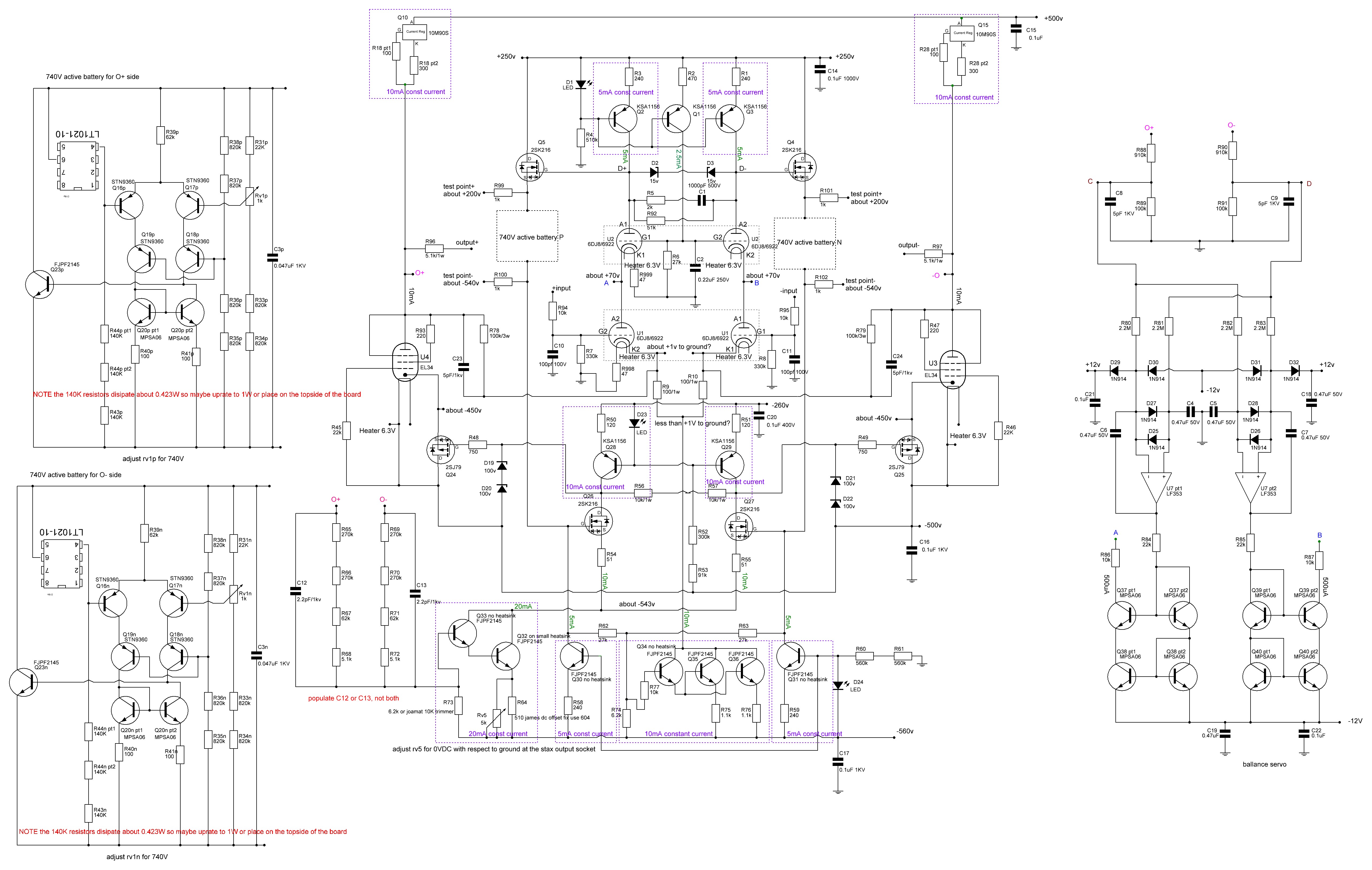
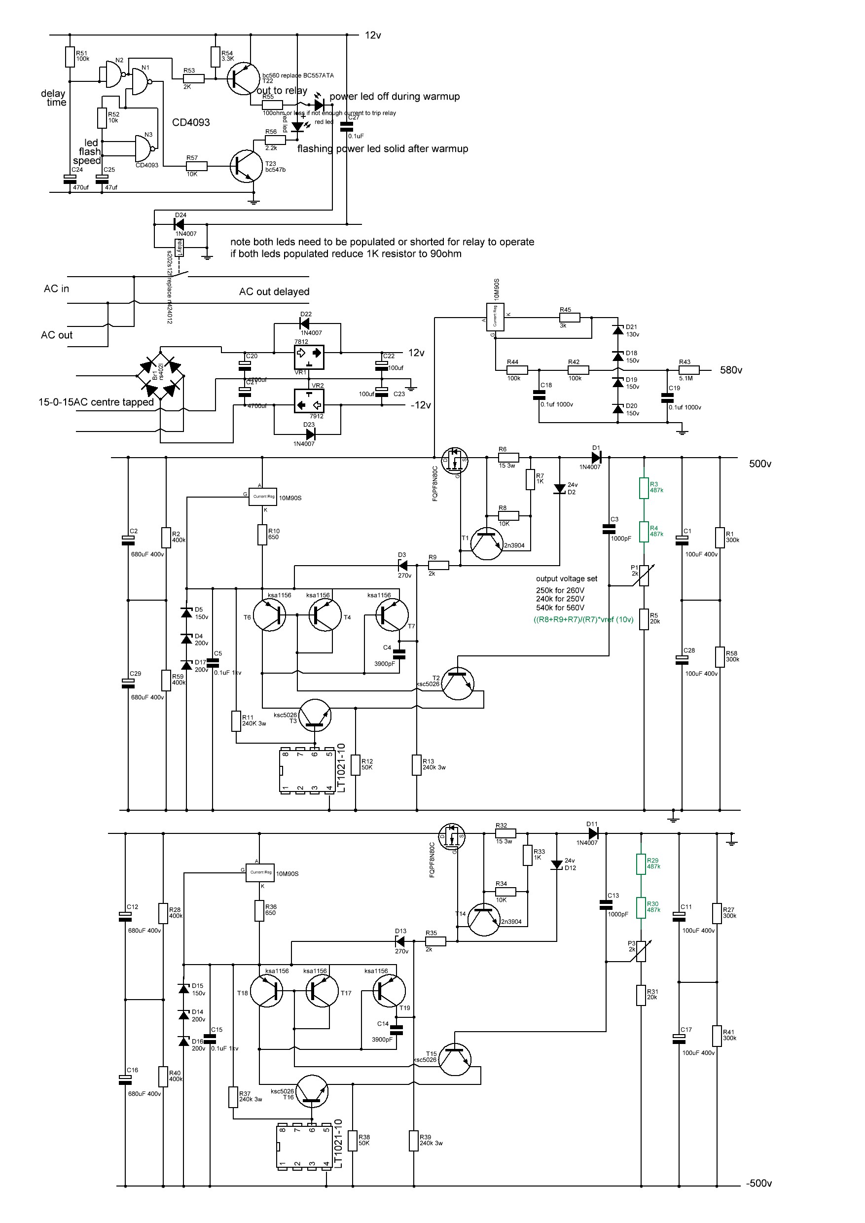
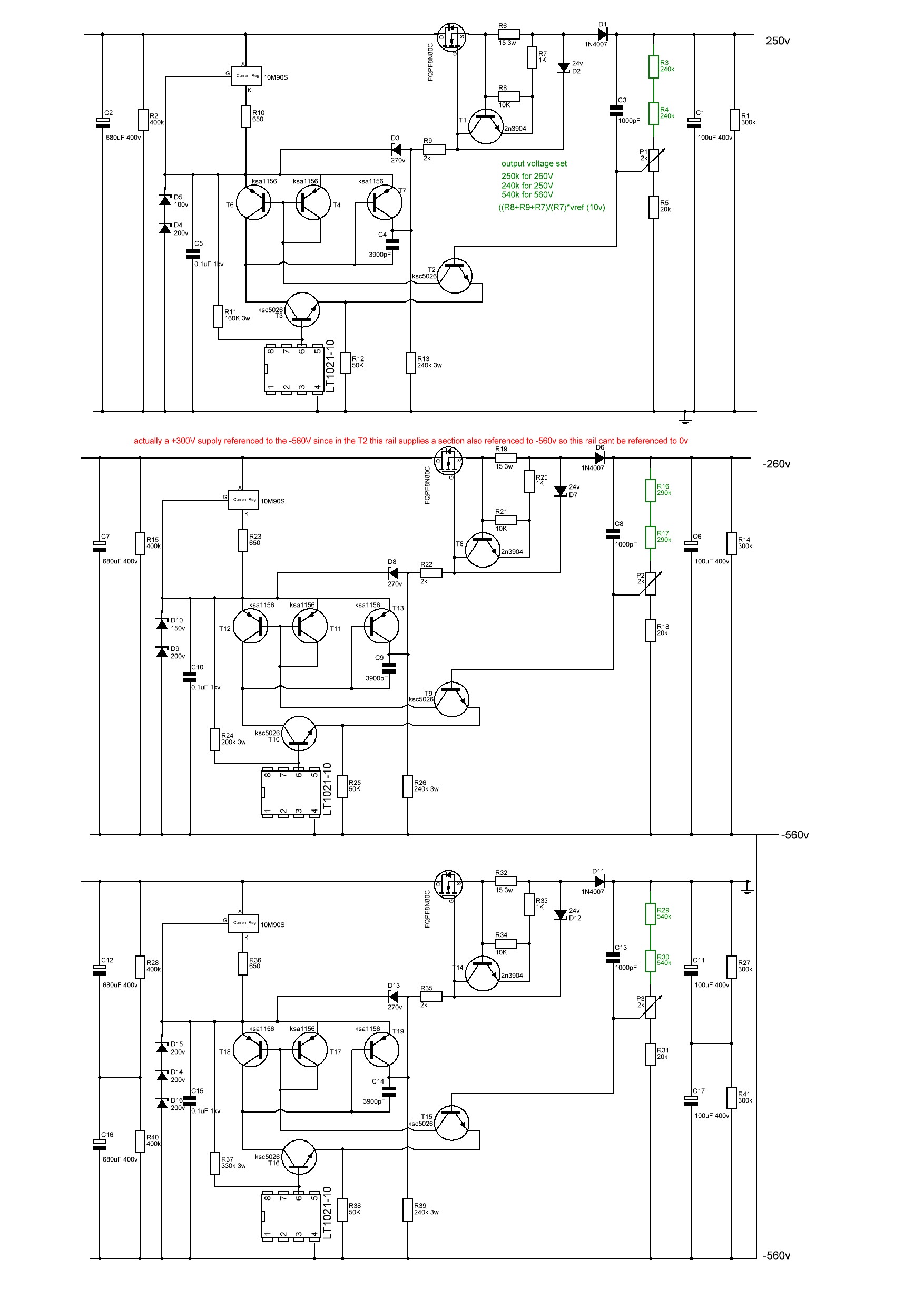
 1 point1 pointIt might be a little premature but I think I now have a working T2 using a modified version of joamat's staxt2nc3fdh7 amp files and kgsshv dc supplies.... Initial startup looks good. Channels started up seperately. Heater transformer running at full voltage. High voltage transformer on a variac. virtual batteries within 100mV of 740V before any adjustment. DC balance between + and - sides of a channel <1V without any adjustment, all 3 leds lit on both channels. once my hands stop shaking I will take a few photos... I have been dreading switch on... in the meantime here's a few build photos of a finished amp channel top and bottom, the amp and psu I modified the delay circuit on one of the psu boards to use a relay instead of the now unavailable solid state relay. I modified the amp boards so that 1. they fit into a 400mm deep chassis, hifi 2000 dissipante chassis. 2. they have screw terminals for all connectors on the top.. (less neat but easier for testing and rebuilding) 3. all resistors of 1W or more go on the top of the pcb with a drill hole under for increased airflow 4. groundpane is between 1.1mm and 1.3mm from any solder point 5. pcb is cut in half so each channel can be built, tested and mounted independently, 6. solder points for pot and input jacks removed and replaced with screw terminals. 7. silkscreen has instructions for adjustment of pots 8. mpsw06 transistors replaced with mpsa06 9. small standalone heatsink for Q34 FJPF2145 in the 20mA current source darlington pair has drill holes in the pcb by the fins for enhanced airflow. 10 all components have schematic numbers included in the silkscreen 11 leds and adjustment pots mounted on top side of pcb like the original T2 12 removed the bias input and 5.1M resistor (since the kgsshv psu already has the resistor in the bias section) I will be happy to release the gerber files of my modification once I am certain the amp is reliable For the build: wima film capacitors, mixture of koa cm1/2 and xicon 273 series 1/2W resistors, for higher wattage vishay pr02 and pr03 All resistors, diodes, zeners raised from the pcb. pcb 2mm with 2oz traces. All 1/2W resistors matched to 0.1% or better at 1khz on a good LCR meter between + and - sections of an amp board AND between left and right channels. all non psu and psu decoupling caps matched to better than 1% at 1KHz on a LCR meter between + and - sections of an amp channel AND between left and right channels. (except for the pF caps which are just too small to measure accurately). all leds and mpsa06 transistors matched on a dca75 curve tracer between + and - sections of an amp board AND between left and right channels. all zener diodes matched to within 1% or better between + and - sections of an amp board AND between left and right channels. separate umbilical cords for AC heater power and DC voltages all internal wiring 1KV silicon all signal wires will be cardas chassis wire volume pot tkd 2500 series left to do install rca signal wiring, volume pot and stax output socket test with signal generator and measure distortion etc collapse from T2 build anxiety drill top of case for valve sockets clean up wiring pray to the god(s) of electronics sort out grounds on psu post moar pictures Here is the schematic for the staxt2nc3fdh7 NOTE this is my reverse engineer based on the pcb and the original T2 schematic and has not been checked by anyone. ( as far as possible component labels reflect the original T2 component labels. In the case of 2 components replacing a single component in the original T2 the components are now labeled Xpt1 and Xp2. In the case of additional components no present in the original T2 they start with the number 9XX. In addition both batteries are shown and the the components labeled with a Xp for the O+ side battery and Xn for the O- side battery. Note the 140K resistors in the virtual batteries dissipate 0.423W each and I found xicon 1/2W 273 series discoloured and drifted by about 1% after about 6 months heavy use when placed on the underside of the pcb. So you may want to think about 1W resistors or place the resistor on the top side of the pcb. psu low voltage, bias, +500V -500V and hv delay reverse engineered from pcb and original schematic. not checked by anyone. psu +250V, -260V and -560V reverse engineered from original schematic and pcb not checked Note psu schematics changed 22/08/2022. Thank you to Rinat for spotting an error on the current path around the 3900pF cap.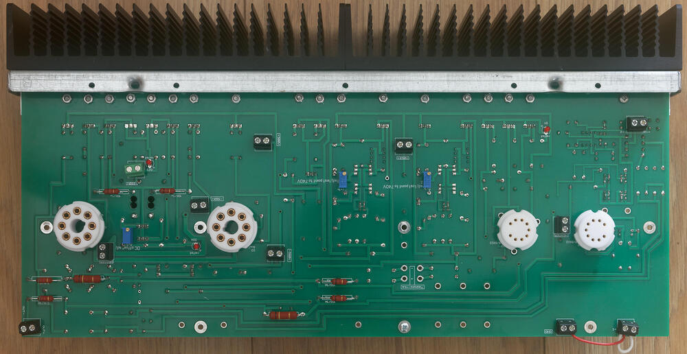
 1 point










.jpg.7a7a58ad25193d491429a27369b1c1ad.jpg)
.jpg.4076fdc721aa36a1e244a4a89b95d66b.jpg)

Important Information
By using this site, you agree to our Terms of Use.
Account
Navigation
Search
Configure browser push notifications
Chrome (Android)
- Tap the lock icon next to the address bar.
- Tap Permissions → Notifications.
- Adjust your preference.
Chrome (Desktop)
- Click the padlock icon in the address bar.
- Select Site settings.
- Find Notifications and adjust your preference.
Safari (iOS 16.4+)
- Ensure the site is installed via Add to Home Screen.
- Open Settings App → Notifications.
- Find your app name and adjust your preference.
Safari (macOS)
- Go to Safari → Preferences.
- Click the Websites tab.
- Select Notifications in the sidebar.
- Find this website and adjust your preference.
Edge (Android)
- Tap the lock icon next to the address bar.
- Tap Permissions.
- Find Notifications and adjust your preference.
Edge (Desktop)
- Click the padlock icon in the address bar.
- Click Permissions for this site.
- Find Notifications and adjust your preference.
Firefox (Android)
- Go to Settings → Site permissions.
- Tap Notifications.
- Find this site in the list and adjust your preference.
Firefox (Desktop)
- Open Firefox Settings.
- Search for Notifications.
- Find this site in the list and adjust your preference.