

Leaderboard
-
JoaMat
High Rollers7Points1558Posts -
Grahame
High Rollers5Points16721Posts -
Craig Sawyers
High Rollers5Points5495Posts -
EdipisReks1
High Rollers5Points3099Posts


Popular Content
Showing content with the highest reputation on 02/15/22 in all areas
-
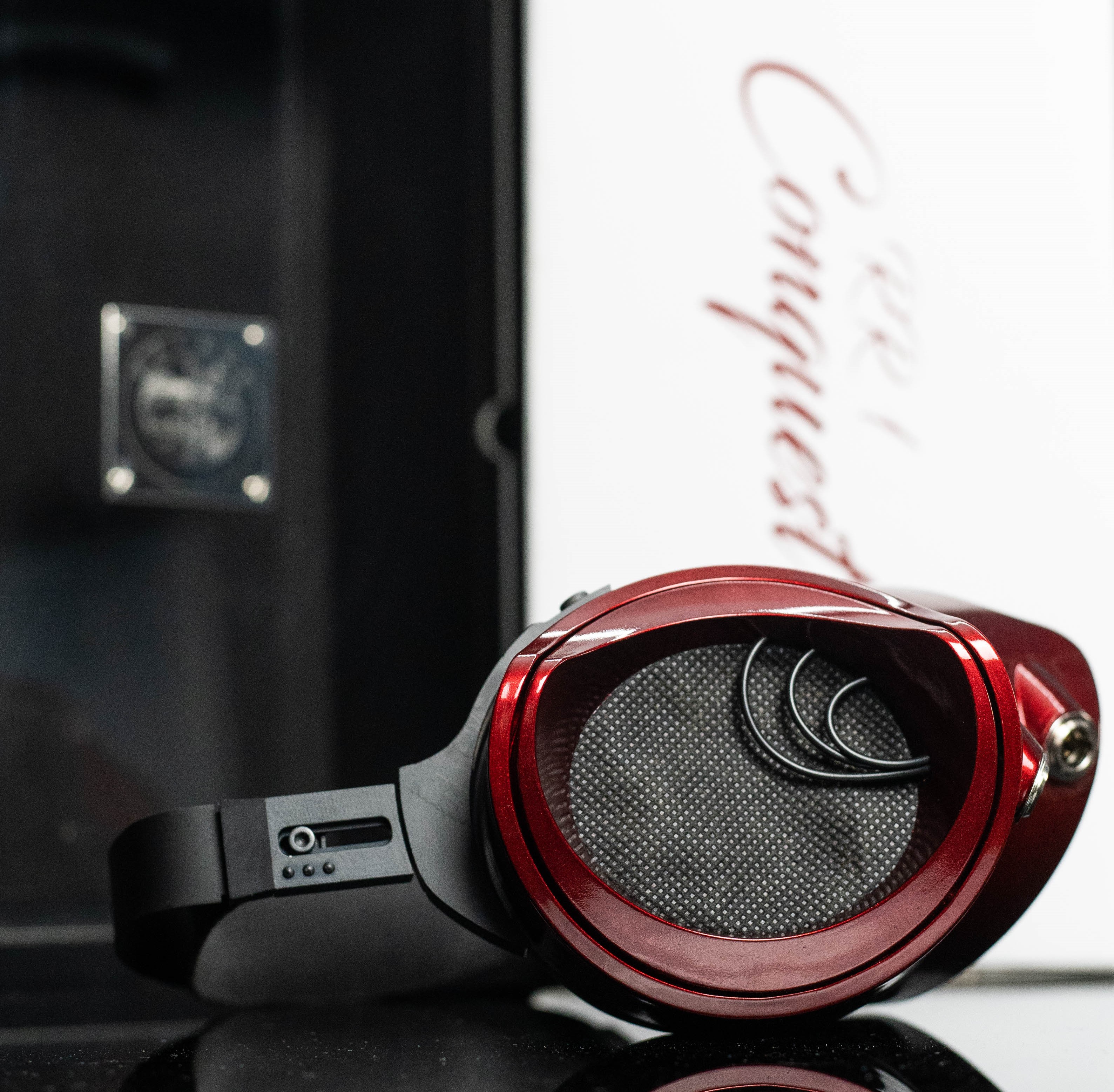
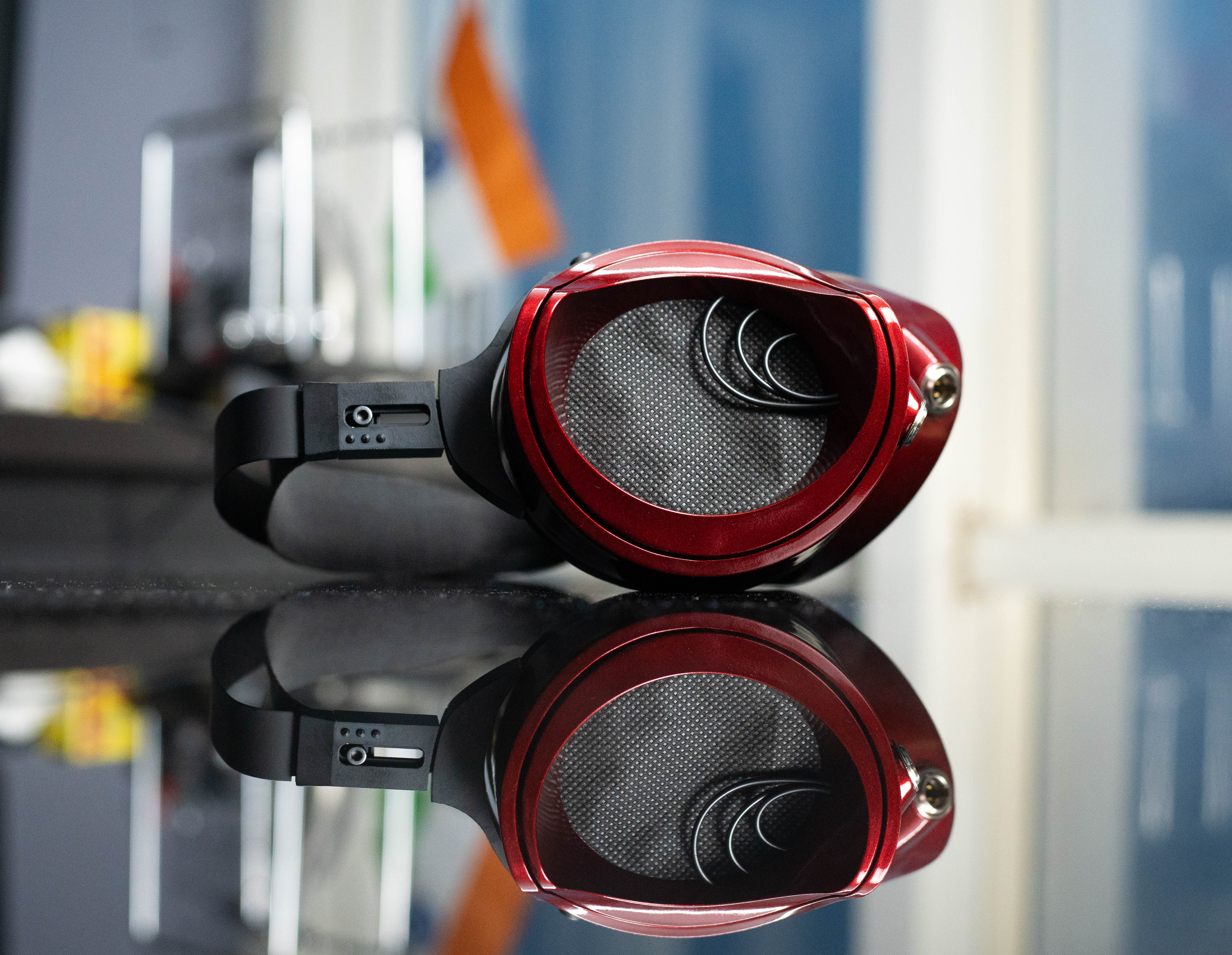
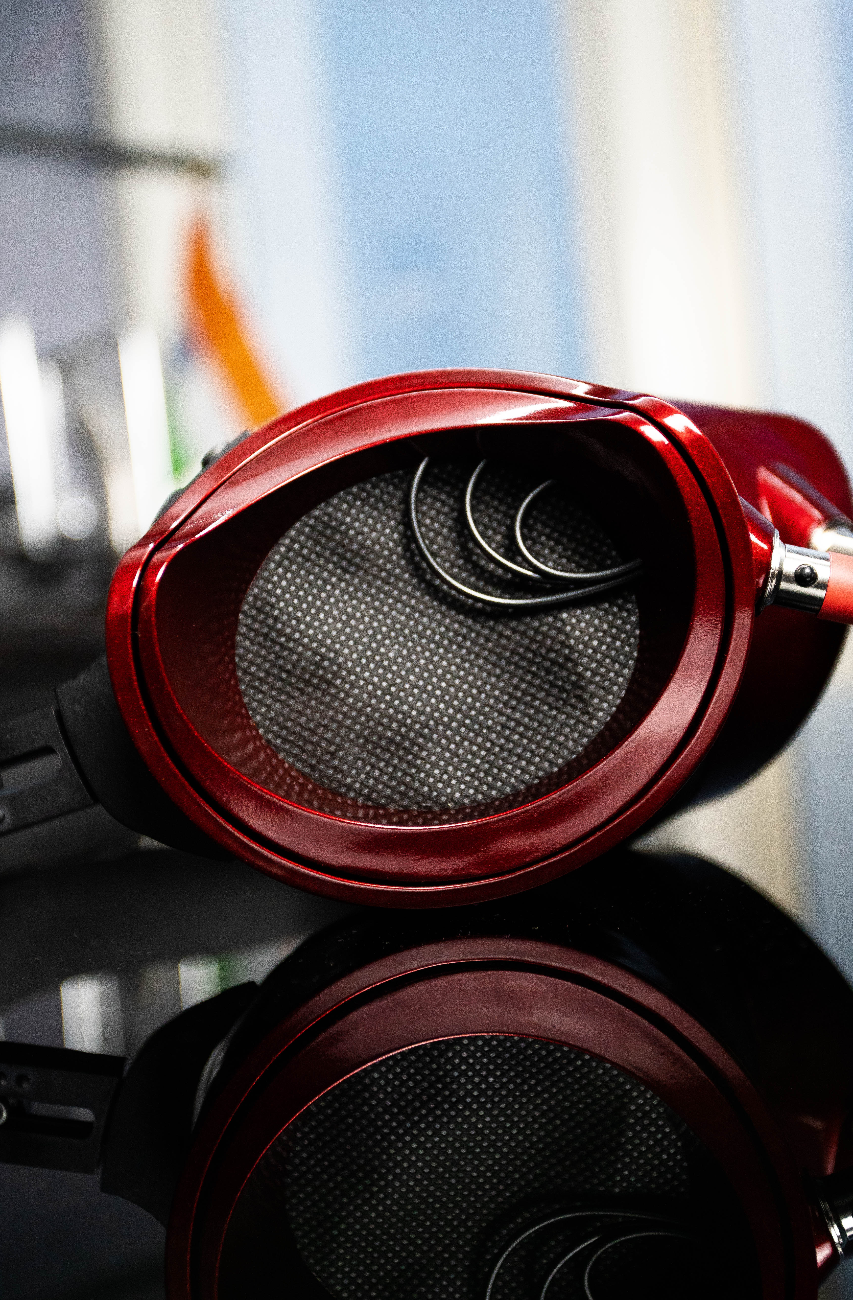
Found another unicorn in this X9000-related article (subscribers only) SR-Omega prototype made out of gold plated solid brass. It's heavy.3 points
-
3 points
-
2 pointsRidley Scott is from my neck of the woods in the North East of England. The beginning of Blade Runner, with the gouts of flame harks back to his walk to school and back in the Winter in the dark. That passed close to the major chemical plants at that time, and they periodically burnt of waste gases in a gout of flame.2 points
-
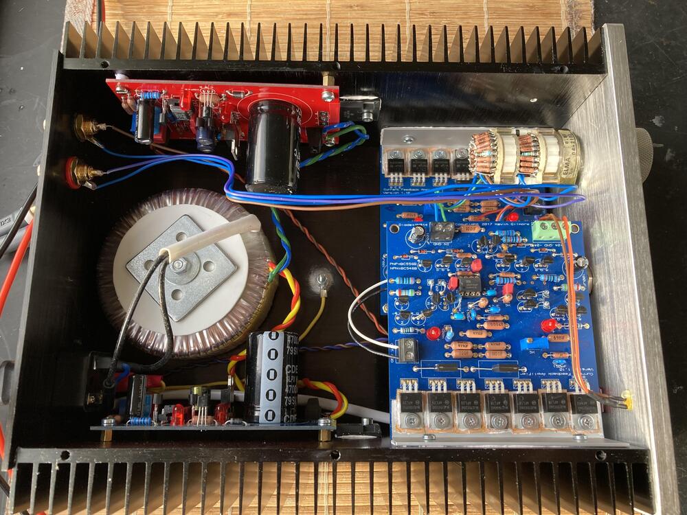
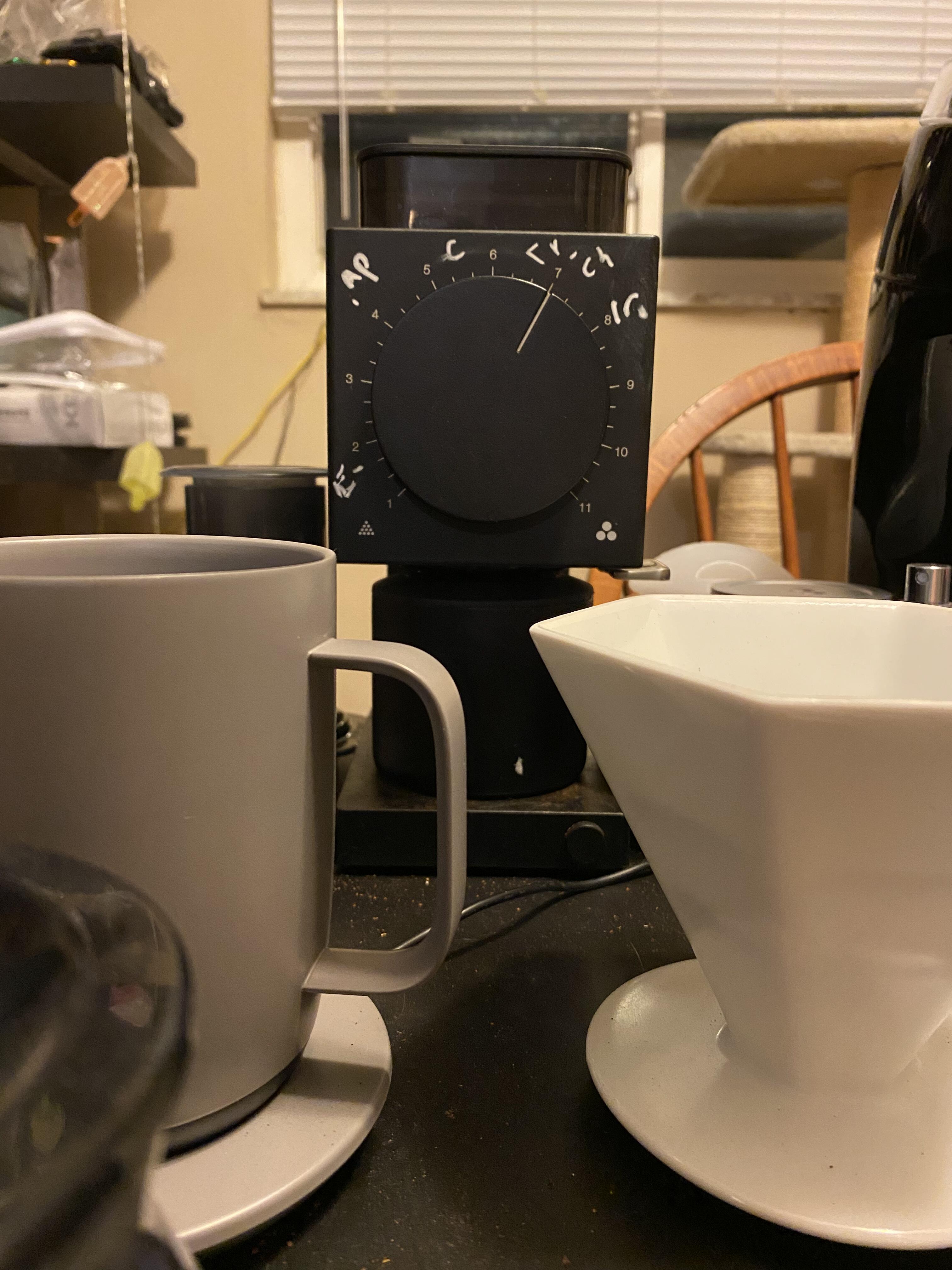
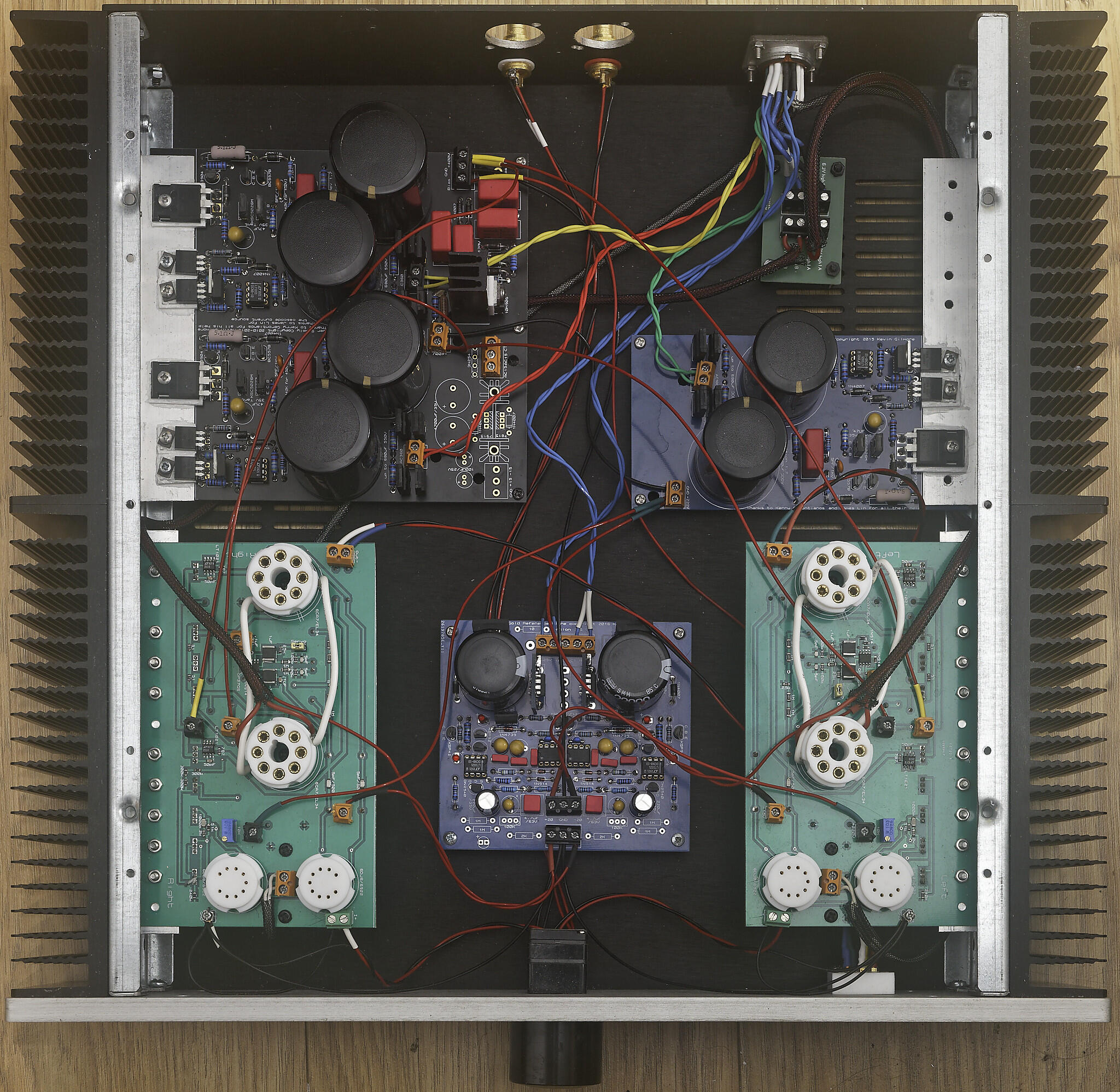
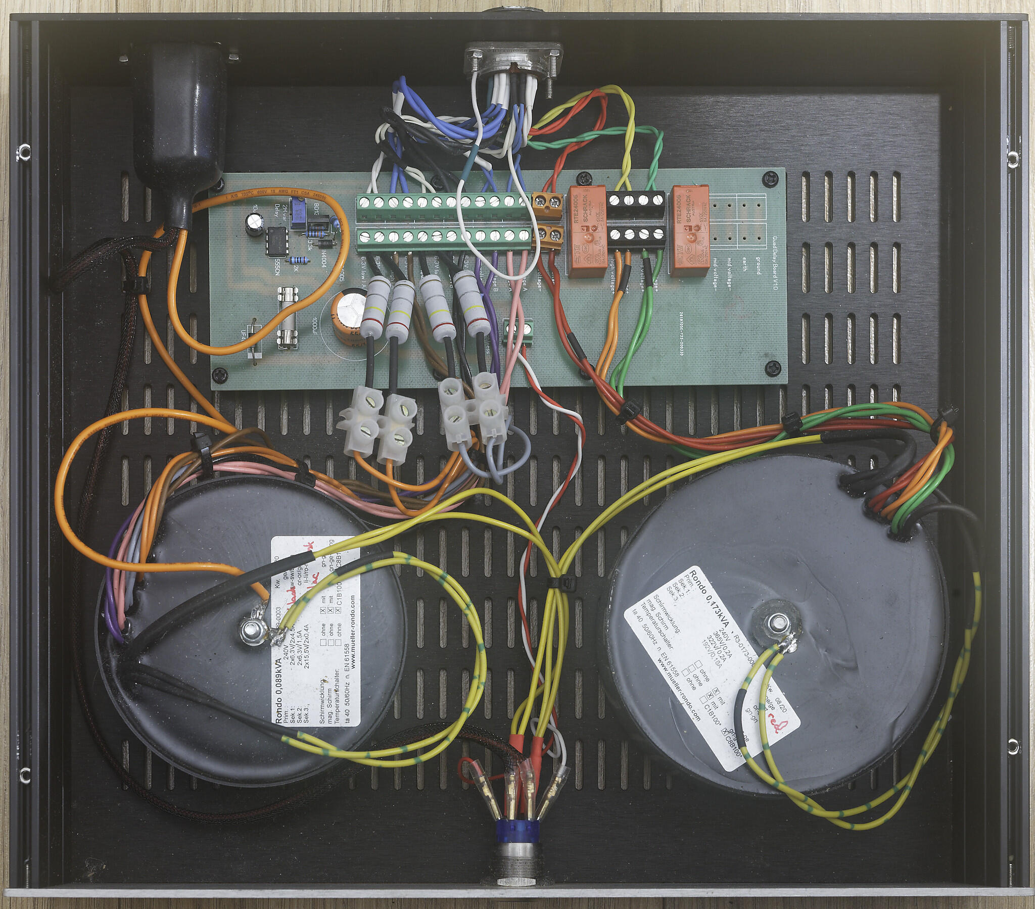
2 points1 point+400 and -460 come from the dual golden reference board, +220V comes from the single golden reference board. look at the amp photo above the dual golden reference is the large square black pcb, the 220V golden reference is on the right hand side of that the blue long slim pcb. The high voltage transformer provides 3 windings, one for each of the high voltage outputs. One wire from each of the high voltage windings is switched by the long thin green delay board in the psu case. if you look at the right hand side transformer that is the high voltage transformer. the colour coding on the transformer wires was green for the 220VDC supply, yellow/orange for the 400V dc supply and red for the 460V supply. To set the outputs of a golden reference hv board you need to change 2 resistors for each output. check the golden reference hv thread for more details. (The 580V bias supply for the headphones is generated from the plus 400V supply.)1 pointI somehow missed this reply completely. The issue with these is that they are in no way Stax compatible. Sure the bias supply might be 600V but for this driver design it should be far higher. Even with the Carbon CC (so more power than you can throw at any one set of headphones) it starts to compress and act up which are the tell tale signs of trying to compensate for a lower bias voltage with the drive voltages. It creates and odd effect so yeah... can't really recommend an amp for these. I need to do a follow up really as there is so much oddity here. I cracked open the supplied headphone cable and wow... it is so weird. Think Hifiman cable but worse... Then we have the energizer which I just rebuilt to my SRD-7 spec. It is just weird, channels swapped and the wiring made no sense at all. Nice transformers but the rest is just utter crap, also unsafe as only the back panel is actually earthed. All 6 panels which make up the chassis are tied to the corner posts, which are made out of plastic so non conductive.1 pointThe Ode is my development grinder. I’m not sure I know what I’m developing, but it’s a good chalkboard.
 1 point1 point1 pointThey work for me. Click on the file icon and a zip file can either be opened or downloaded.
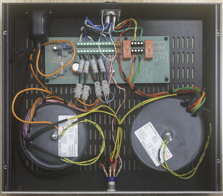
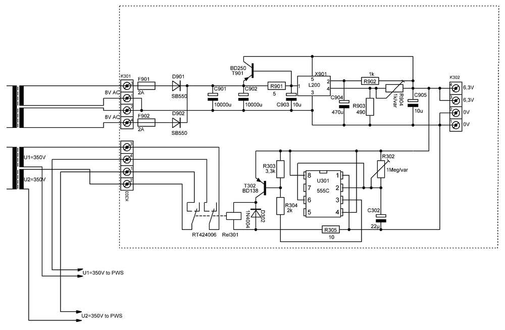
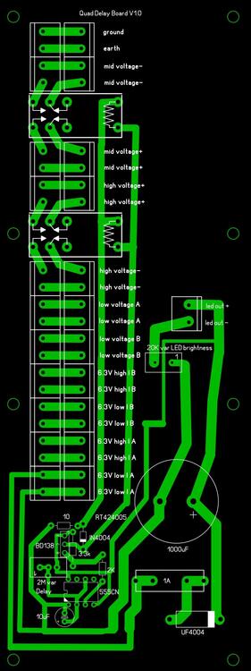
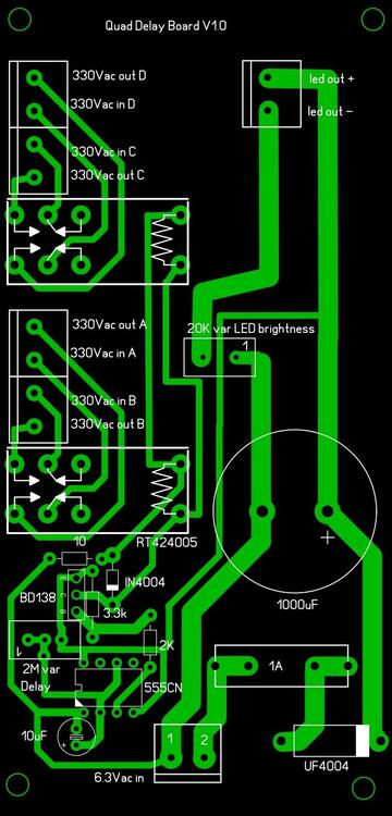
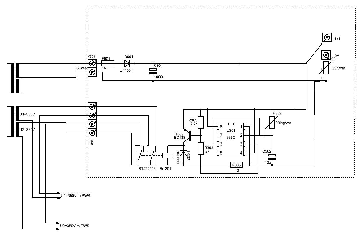
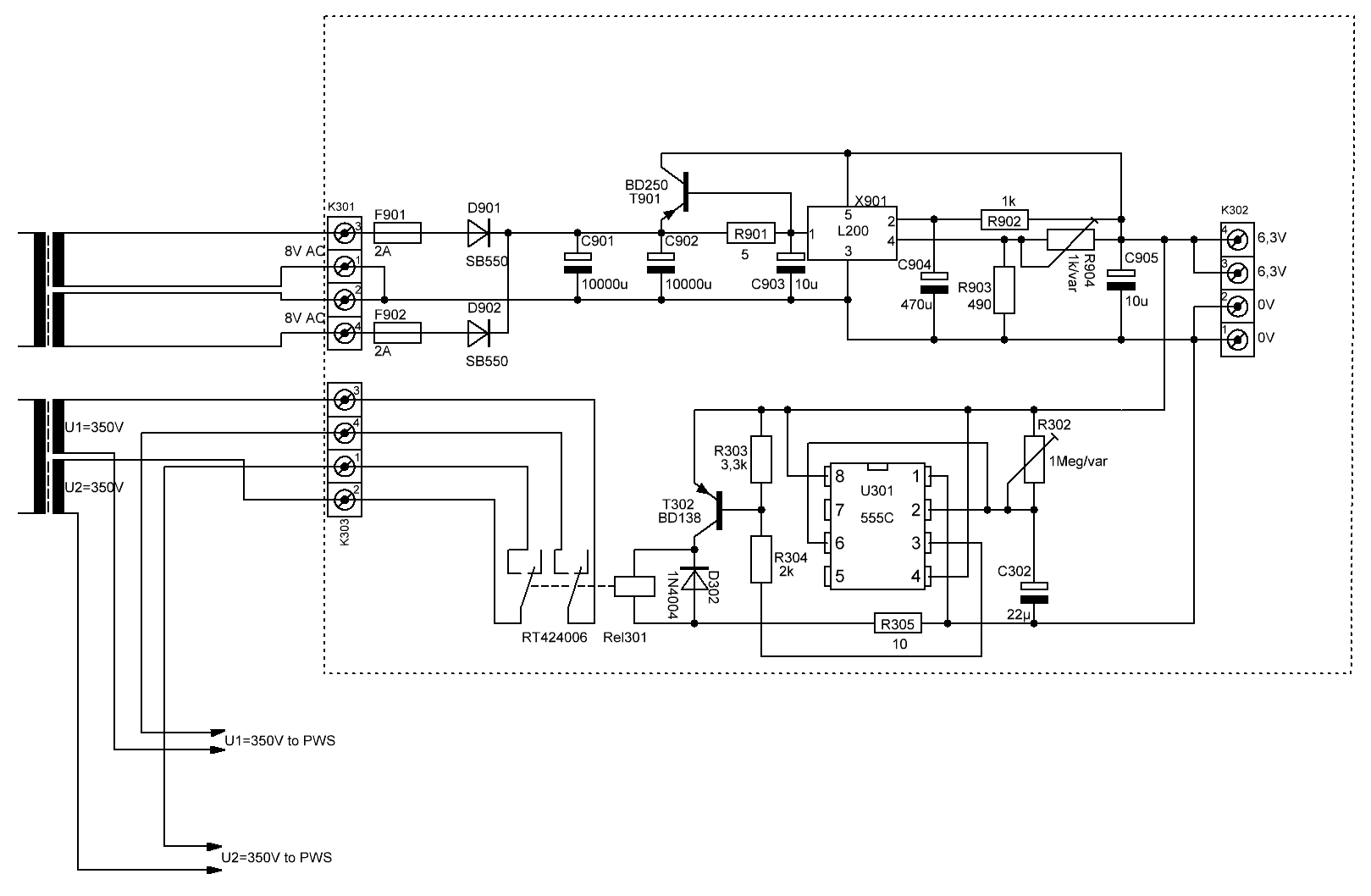
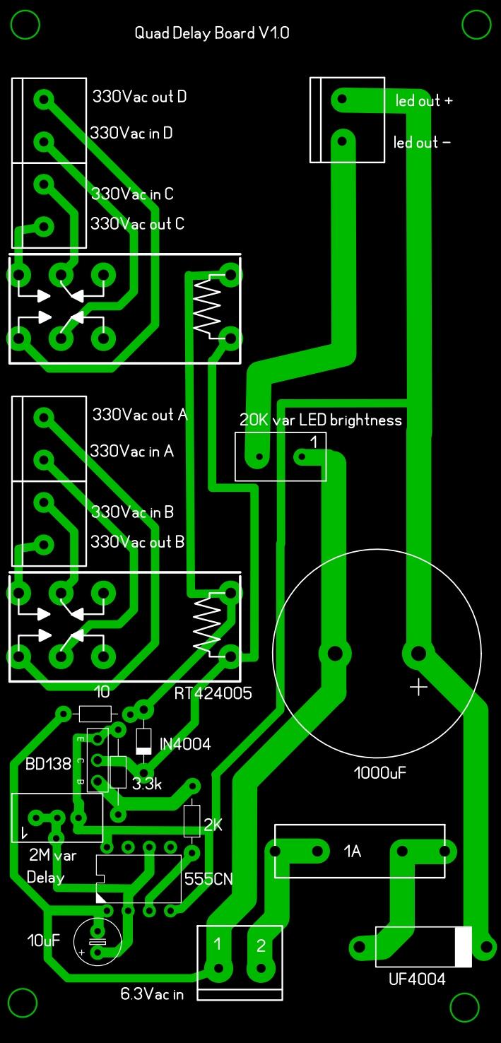
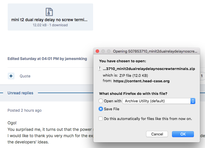 1 point1 point1 pointthere are many possibilities: for the power supplies first you need to decide if you want to heat the valves up before you apply high voltage. If you do then there are two options. Do you want to implement the delay using a relay (and either switching the ac input to the high voltage transformer or dc output of the high voltage psus) or apply a dc voltage to switch on the high voltage psus? IF you do not want high voltage delay or want to do the entire delay e.g. by timed relay off the psu board then use the golden reference 1.7 series psus if you want to switch on the hv psu by providing timed dc then use the golden reference 1.8 boards. next you need 3 hv rails - two positive (220V and 400V) and one negative (-460V). So you need to look at the options. golden reference Dual boards have a positive and negative rail, headphones bias and a simple low voltages + and - rail on one pcb but are of course wider than a single rail board. or you could go for three single rail separate golden reference boards. boards with left in their name have a negative rail and simple low voltage supplies. boards with right in their name have a positive hv rail and the 580V headphones bias. See https://www.head-case.org/forums/topic/15634-goldenreference-high-voltage-power-supply-grhv/#comment-851207 for board physical sizes. Next for an over kill design you may want to have a high performance low voltage section using a golden reference LV board instead of the basic low voltage section provided on the golden reference hv boards. The low voltage provides power to the dc servo, balance servo and cathodes of the 6922s that the input signal goes into for the delay board you can use https://drive.google.com/drive/folders/1r3g2TAtBUaBdiMorTWX7yYgeJ7maQbYW or use what I use which is taken from a German website: schematic: http://www.high-amp.de/html/reg_pws_v3_add_on_schematics.html gerbers etc http://www.high-amp.de/powersupply_stabil_add_on.rar NOTE the hi amp delay board also provides a dc 6.3V supply capable of powering the 6922s but then requires 2 windings of about 8VAC rms as its input. Or you can just not implement the circuit for the 6Vdc heater supply and run the delay timer and relay off a single 6.6VAC winding without issue - which is what I do (see bellow). If you only implement the delay from the high amp board this is the schematic of what you need: Here is my build with a golden reference HV 1.7 dual and golden reference 1.7 right (modified by me to remove the bias components), and a golden reference lv (the delay board is in the psu box with transformers.). The delay board I designed myself based upon the delay circuit from high-amp. It runs off one of the 6922 heaters and is modified so it switches all three outputs of the HV transformer - which is why there are two relays. It also provides screw terminals so you can attach dropper resistors if your heater voltages are two high. (I like to run the heaters 6922s at 6VAC rms). The delay board I made also provides dc power for the led in the on off switch. Removing the fuse allows you to power up the heaters and low voltages only. The standard hi amp delay board only provides a single relay which can be used to switch the AC input to the high voltage transformer. This mandates the use of two transformers - one for the low voltages, heaters and delay board power and a separate one for the high voltages. My board switches the outputs of the HV transformer and so could be used with a single transformer setup or dual transformers. It also provides terminals for all voltages going to the amp. (I have a build policy that all pcbs and major components e.g. transformers should be removable for servicing with zero disordering - hence the screw terminals added to the delay board.) here is the gerbers for my dual relay pcb with screw terminals: mini t2 delay with screw terminals.zip here are the gerbers for the dual delay with no extra screw terminals for the other voltages: mini t2 dual relay delay no screw terminals.zip
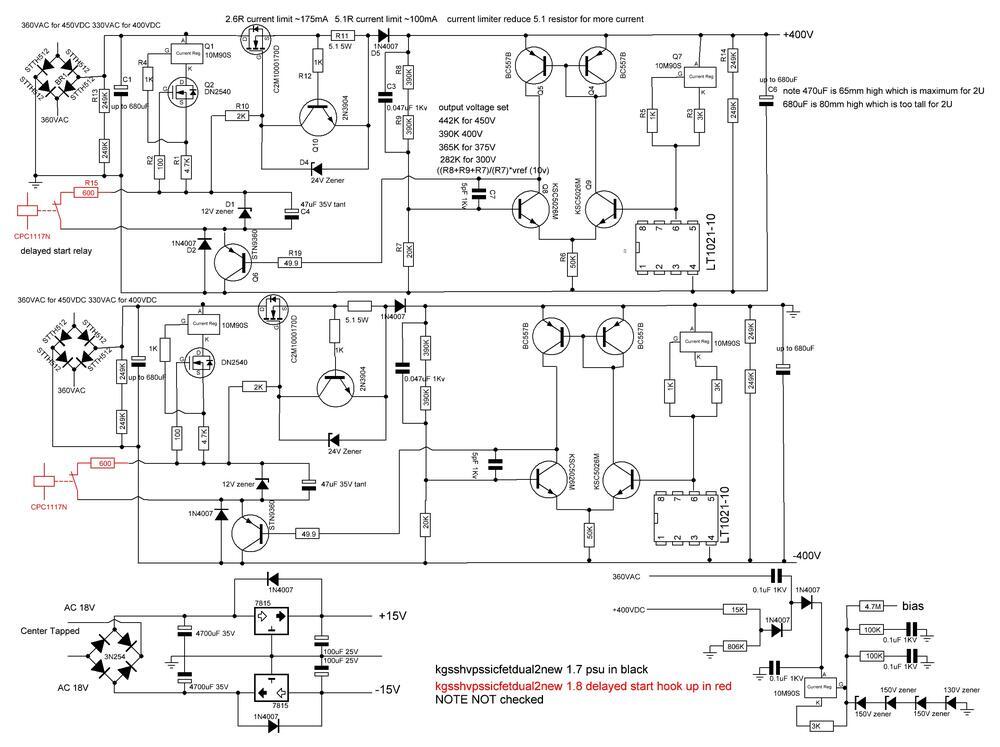


 1 pointso split versions of the cfa3 board. stack the boards together and put on the heatsink (minimum heatsink vertical dimension 83mm) stack the boards together, use angle bracket mount horizontally for low profile chassis etc cfp3smt2splitamp - CADCAM.ZIP cfp3smt2splitpre - CADCAM.ZIP
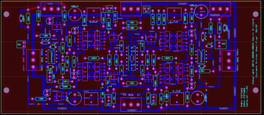
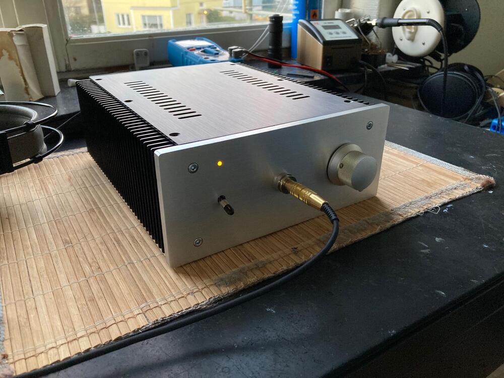
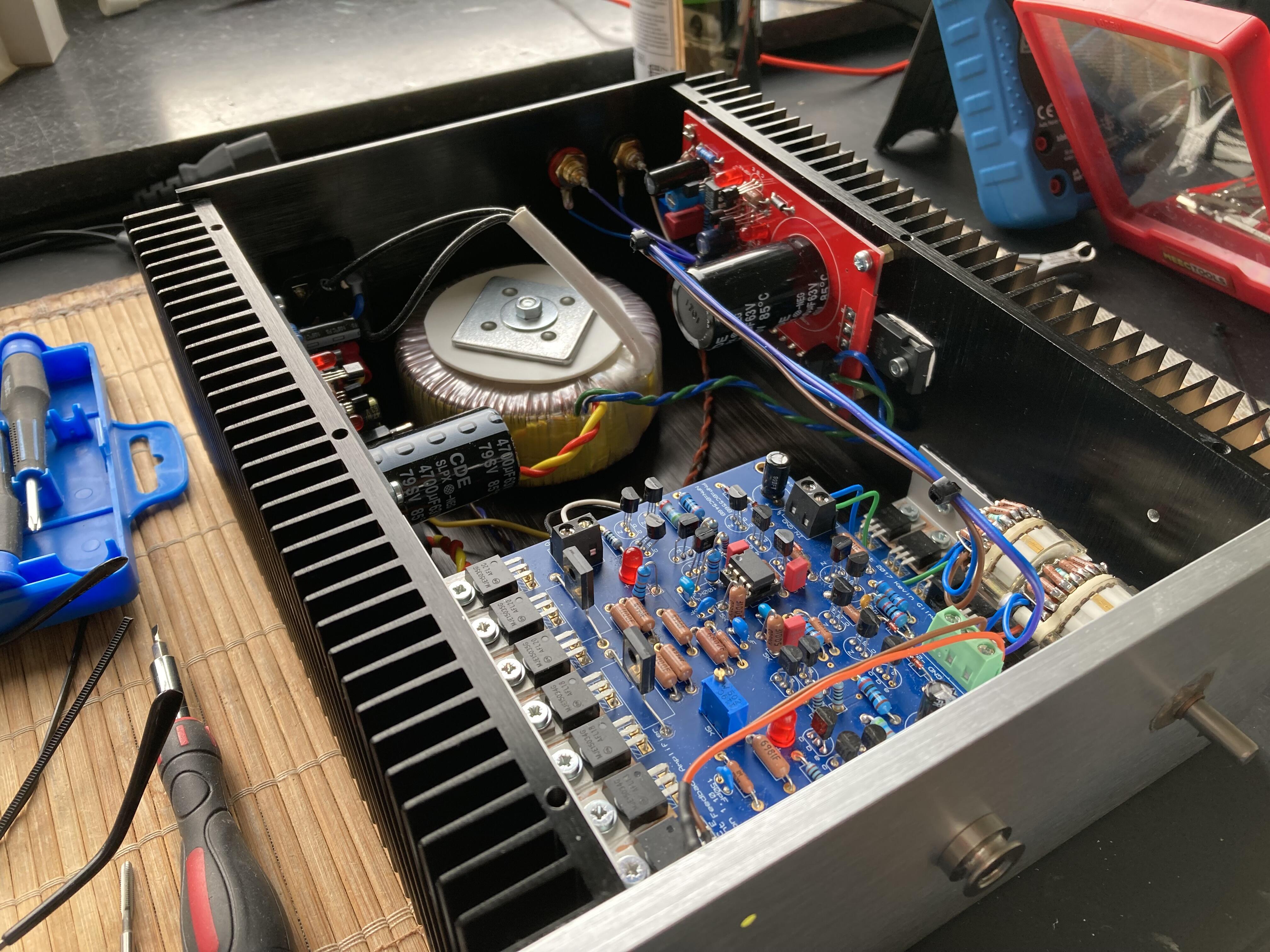
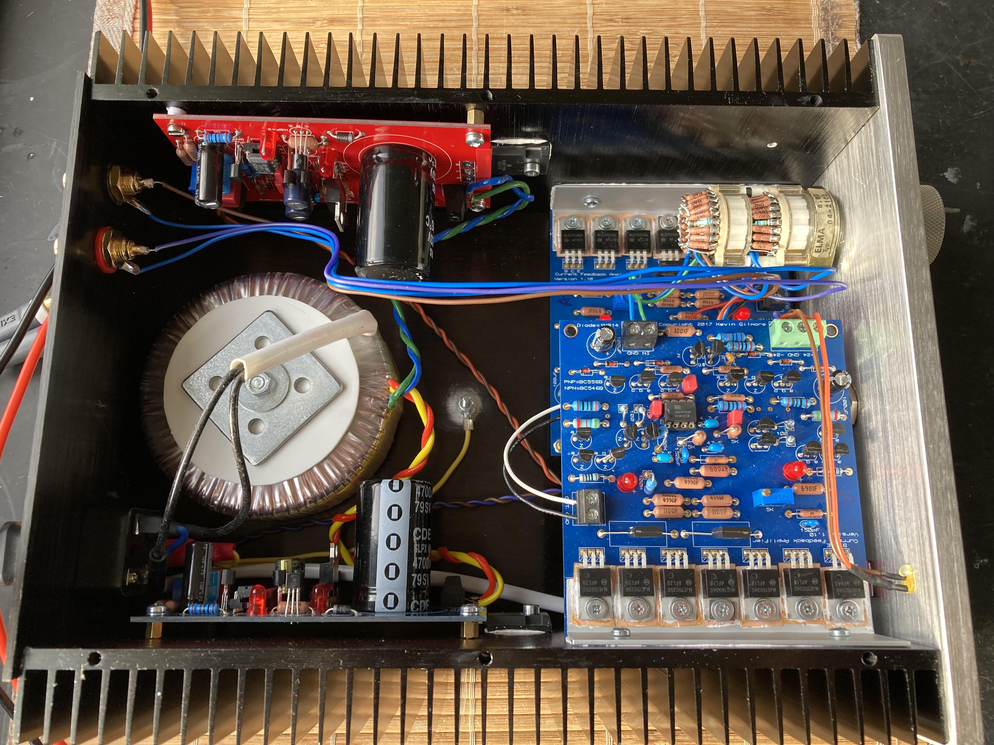
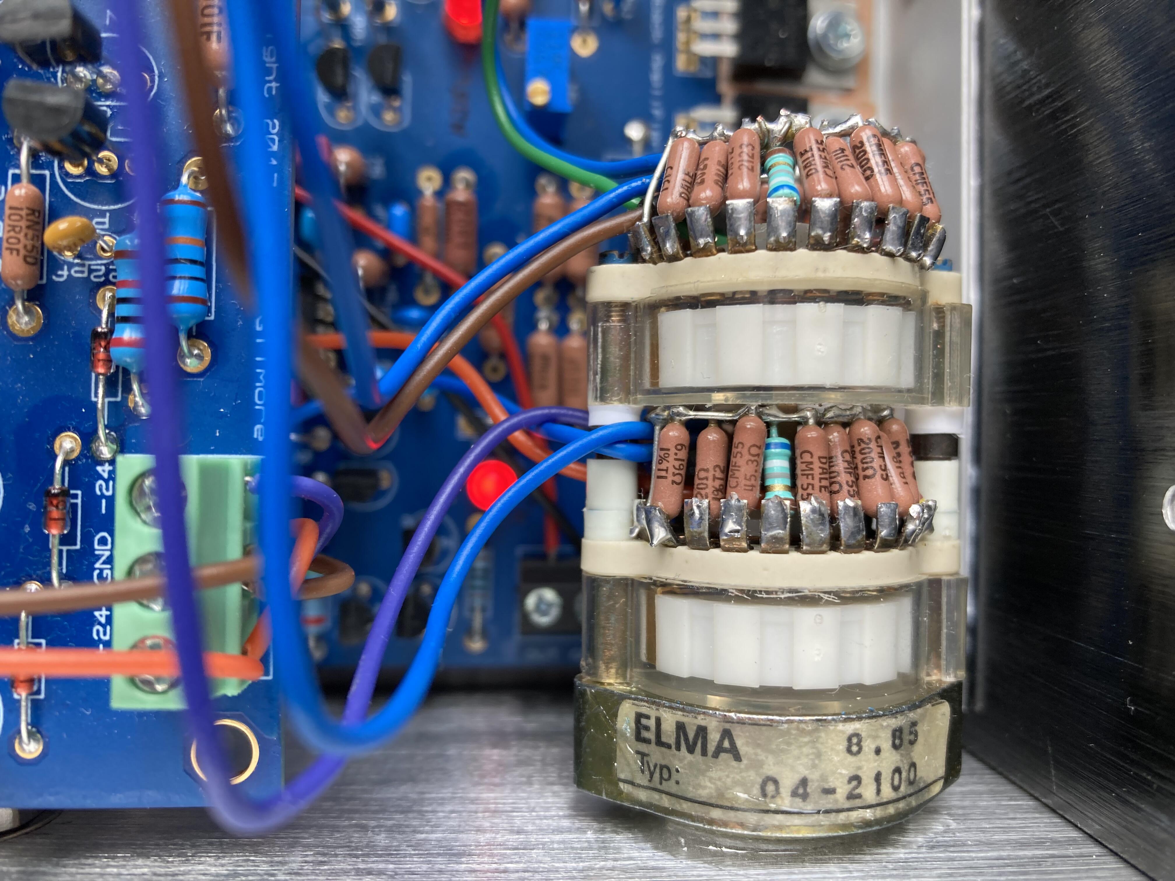
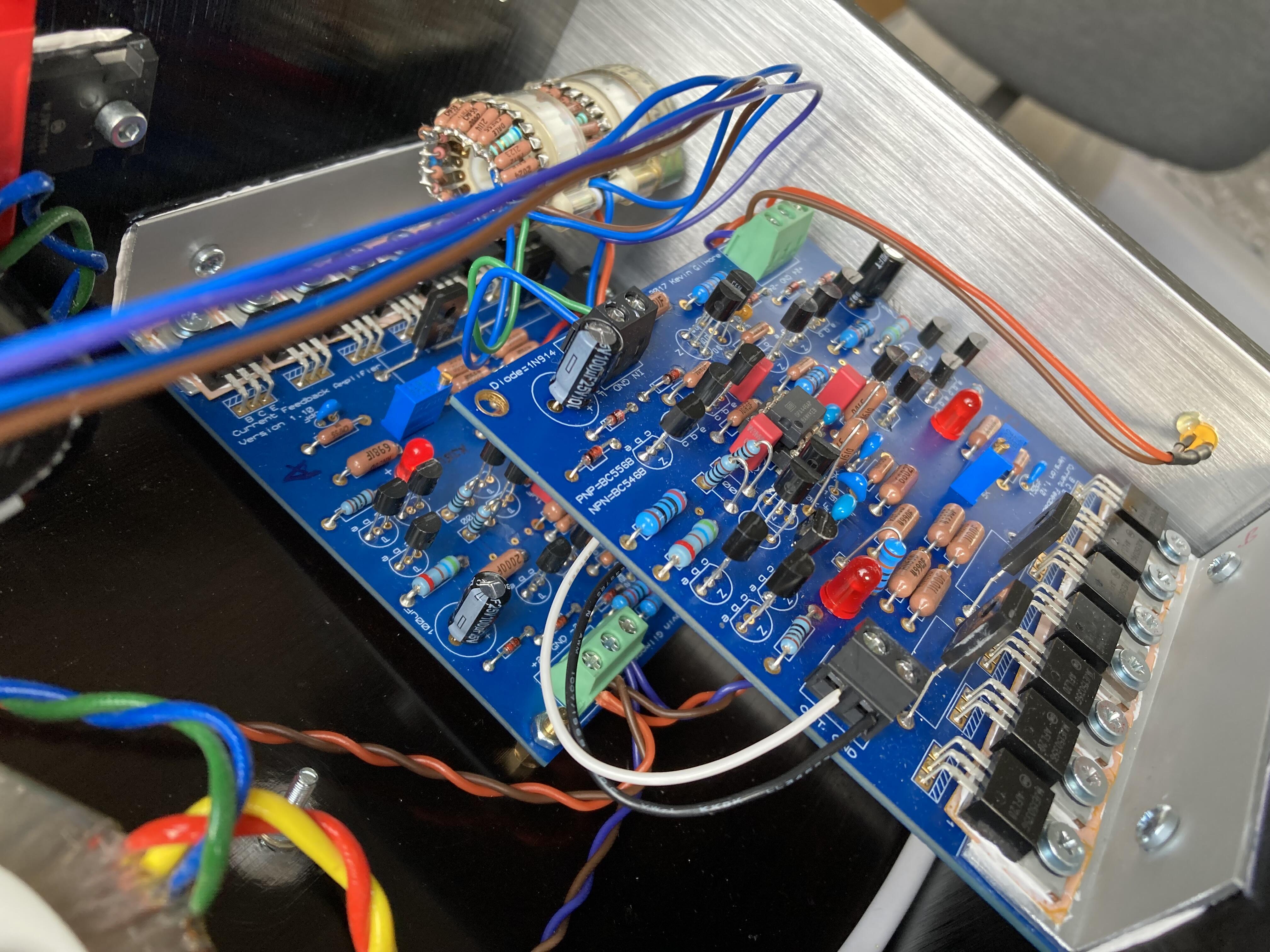
 1 pointLate to the party, but here goes. Lured a nice small case off of MLA for a cheap penny, wanted a compact CFA (SE). Took some time for my slow mind to figure out how to best use the space in three dimensions, but I found a solution that works fine so far, if you're planning something similar. No interfering leads or unwanted nearness of critical components, and bias can be set without problem. In reality, I'm surprised it turned out quite airy and spacious, considering the limitations. Note the Müller Rhombus transformer device ("Konzept Raute"). This romboid plate interacts wit the circular toroid shape and the electromagnetic waves are forced through the four holes in an endless loop in this electronically confined space, and thus traps all hum in an existant/nonexistant void. This amp is noise and hum free. I'm particulary happy with the volume control, a 24-position Swiss Elma switch that's been lying in a drawer for 35 years. 15K (why not?), shunt coupled and making as little contribution to the signal as possible. I think this plays a part in the clean, revealing sound of the CFA design. The odd resistor out is in the position I mostly listen to, a hand selected Syldavian military plutonium component (0,01%) from 1953, made in a numbered series of three of each value (I own the third one as well) and these days sold on ebay in Hong Kong for not less than $1200, if available at all (only one for sale during the last nine years). Set the bias at first to 150mA, it sank to 135 after some time, which was to be expected. Decided too raise it (why not?) to 200mA. Put the lid on and after three hours it was stable at 175mA after a last fine-tuning. Gets warm, but not too hot. Like all successful, completed builds it sounds wonderful , but if that lasts only time will tell. If so, I may be tempted to follow up with a CFA3.
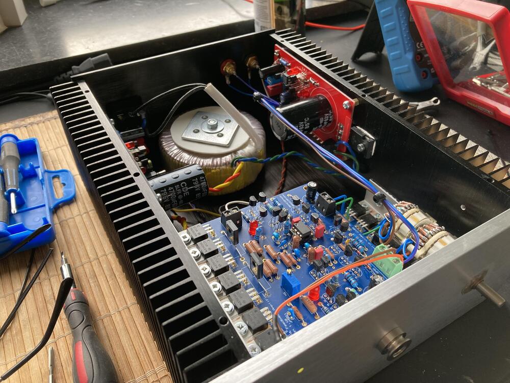


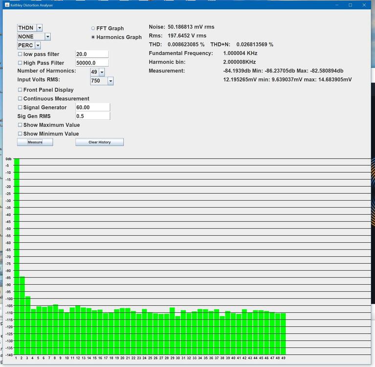
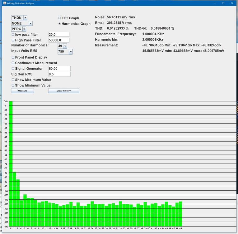
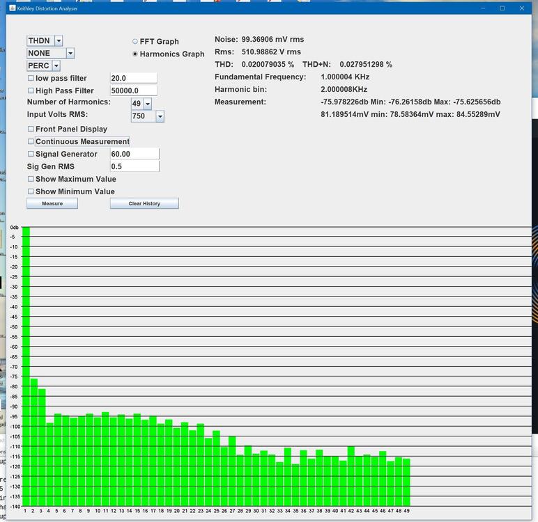
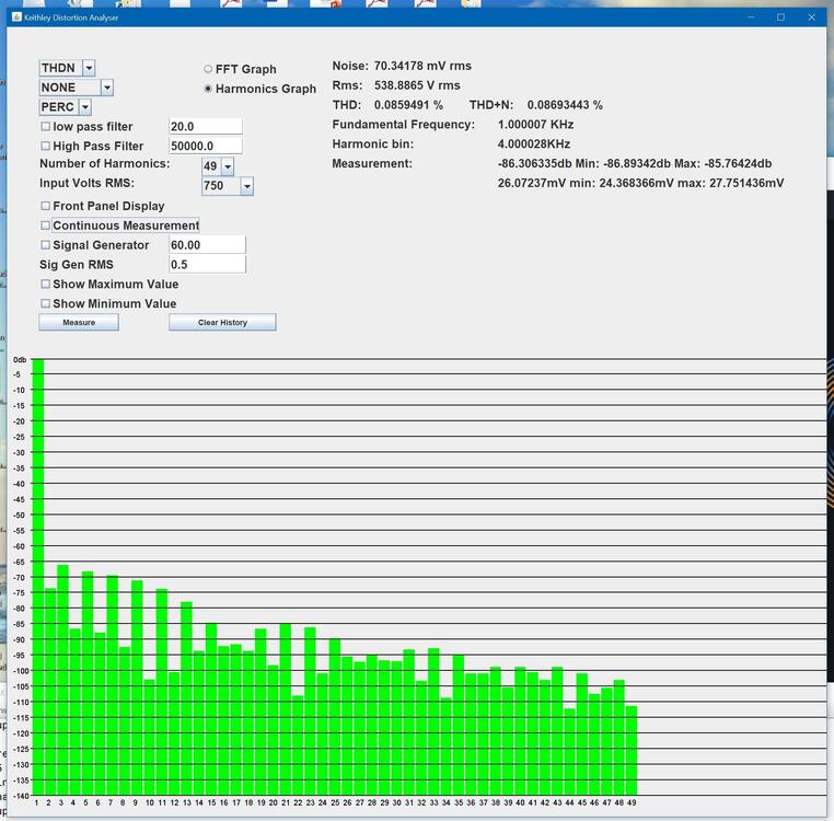
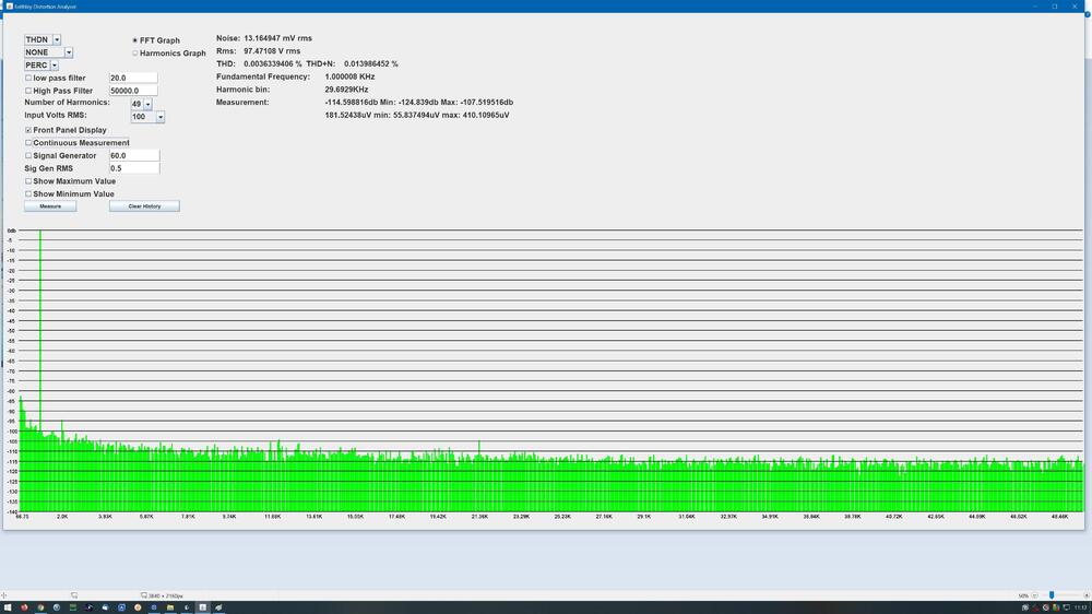
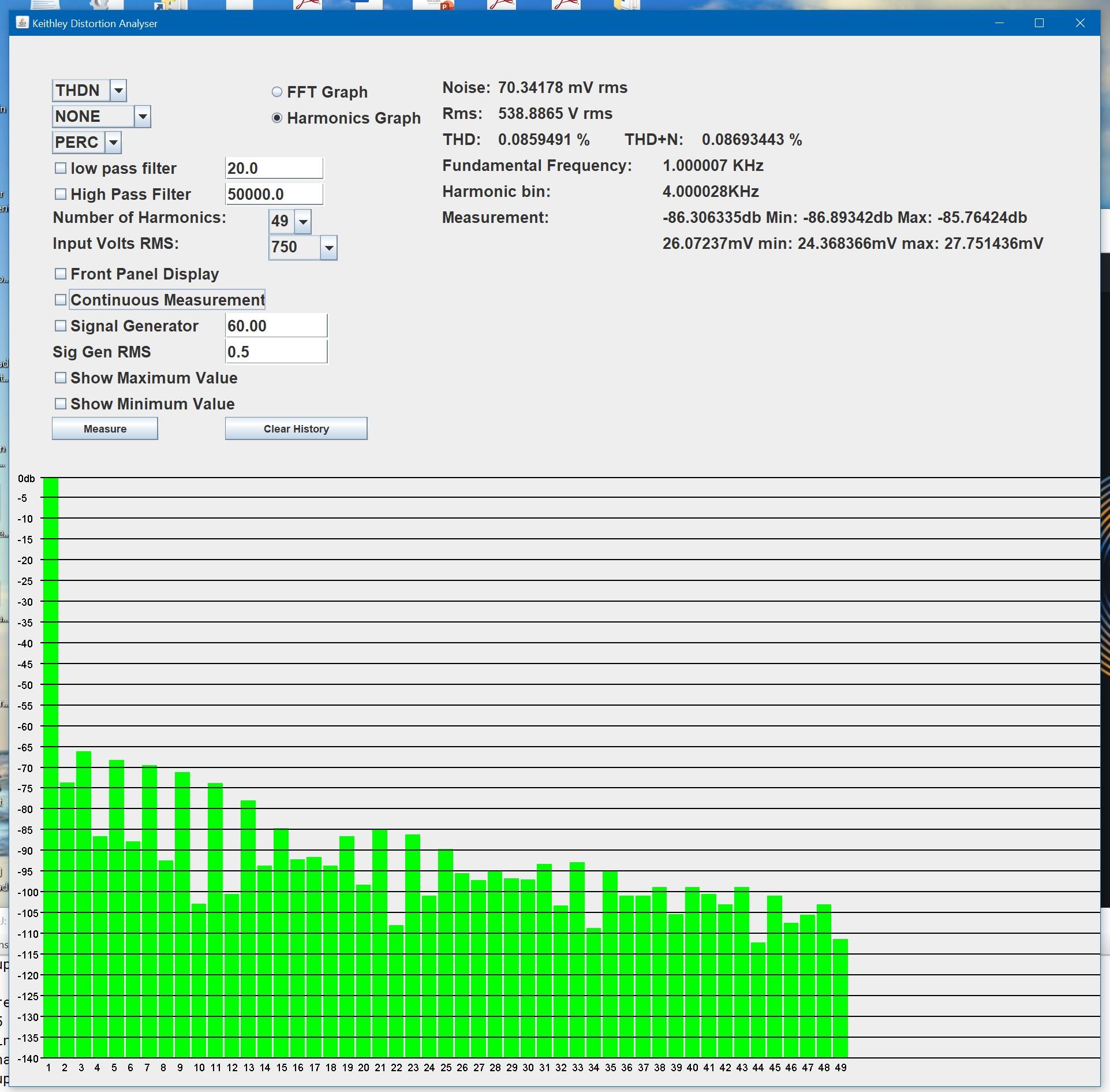
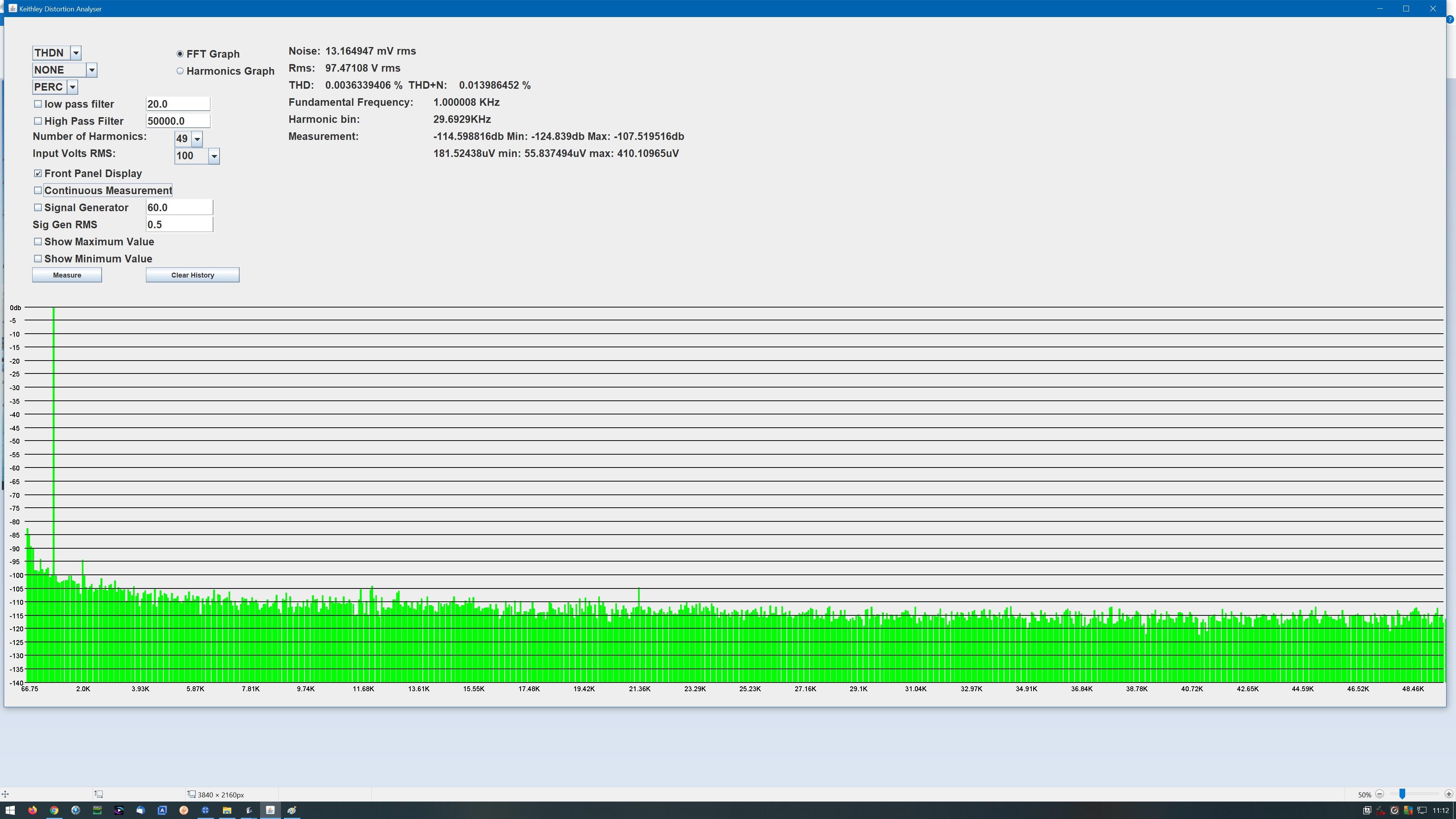
 1 point1 pointLately the left channel humming has increased to become even more bloody annoying. But… today I cured it (pure luck - trial and error approach). I have two umbilicals between psu and amplifier. Both carrying 580V bias and then joining at the stax connector. So, I removed left 580V bias wire in amplifier and the hum disappeared. To my ears the amplifier is now dead silent.1 point1 point1 pointHere are some distortion figures and harmonic analysis up to 50Khz. Test setup groove tubes el34 matched, electro harmonix gold pin 6922 matched, 1Khz sine from a 192K 24bit rme soundcard spdif out to a v90 dac to the mini t2 inputs, measured on a keithley 2015thd. distortion graph is the average of 20 measurements. All other readings are not averaged: Distortion is less than 0.02% up to 500V rms output with second harmonic being the highest and a little bit of third above the noise floor. At just under 500V the 4th harmonic is above the noise floor, above 500V rms clipping starts and at 600V rms distorion is ~2.5% with the second harmonic at -36db relative to the 1khz signal level. On the right hand top side of each graph under the measurement section is the measurements for the 2nd harmonic in db and mVolts average, min and max over 20 measurements. Noise is the ac voltage not in a harminic bin (i.e. a bin which is an integer multiple of 1Khz). Analysis is with 749 bins going from 20hz to 50khz. A full fft with all bins is included for the 100Vrms output only at the bottom of the post. I wrote the software myself, its very much a rapid prototype kludgy mess but I hope to make it available to community members with keithley 2015 when the code is not so offensive. At the moment there is no guarantee that it will not open up a dimensional hole and make all your original NOS Japanese transistors disappear. FFT analysis 1Khz 100Vrms output. 20hz to 50khz


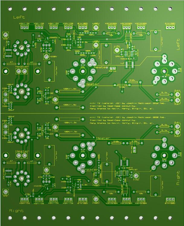
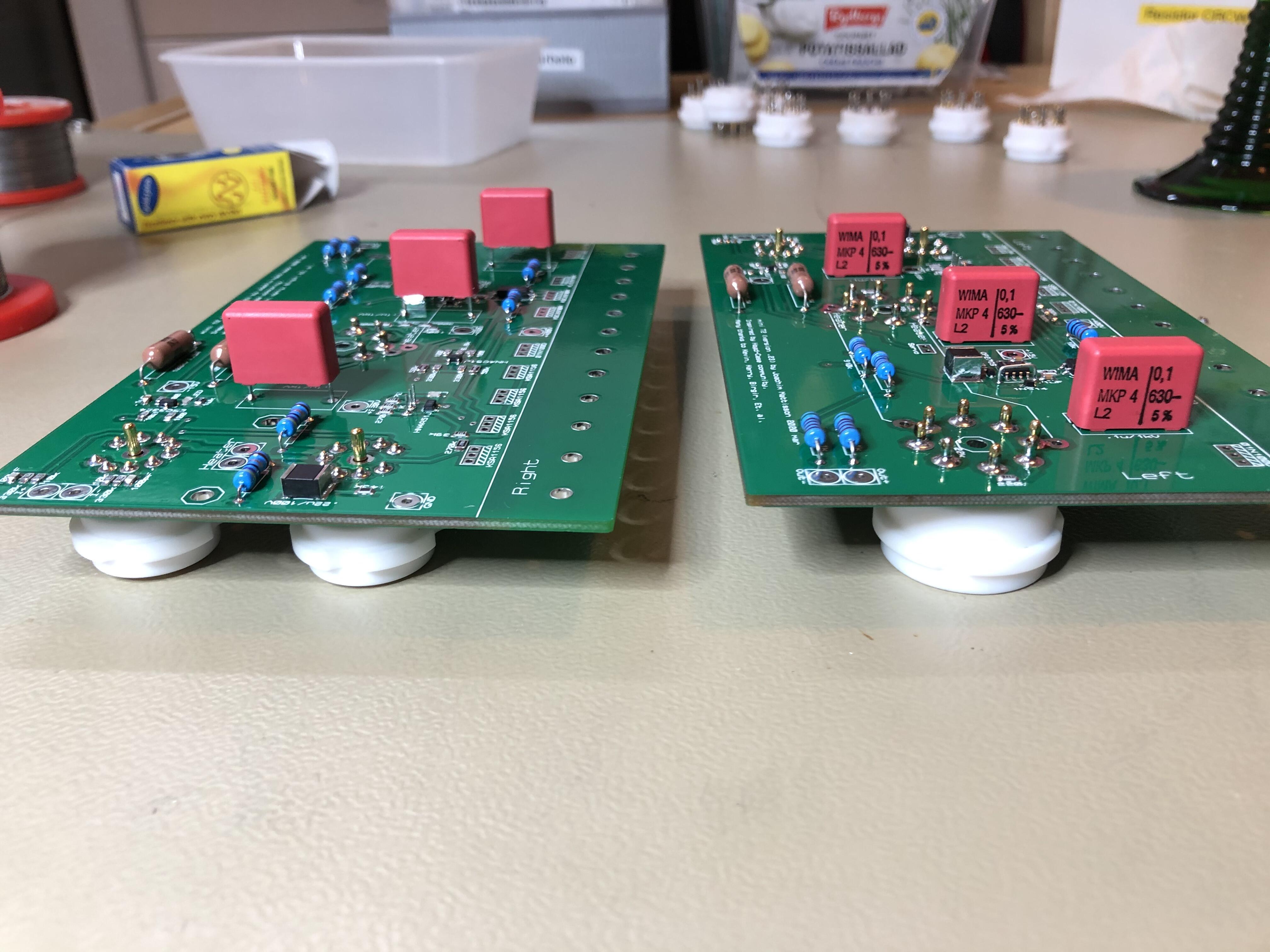
 1 point1 pointNow completed mini T2 with the new boards version .23. Squeezed in film caps with 0.8 mm leads on right channel with 0.76 mm hole diameter, elevated and soldered both sides (see below). Both channels worked right away. Only issues I’ve found with those new boards are mentioned in posts above.
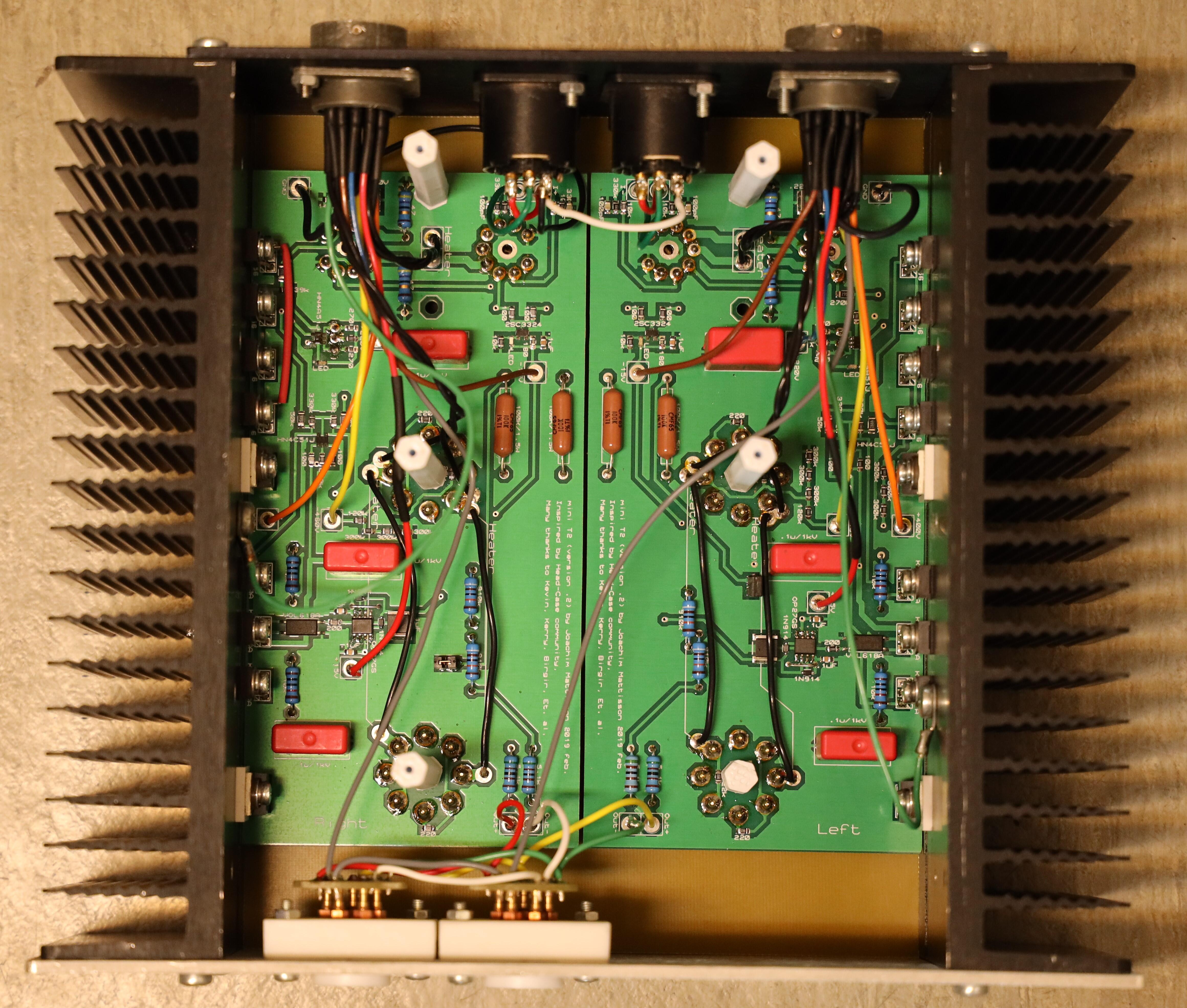
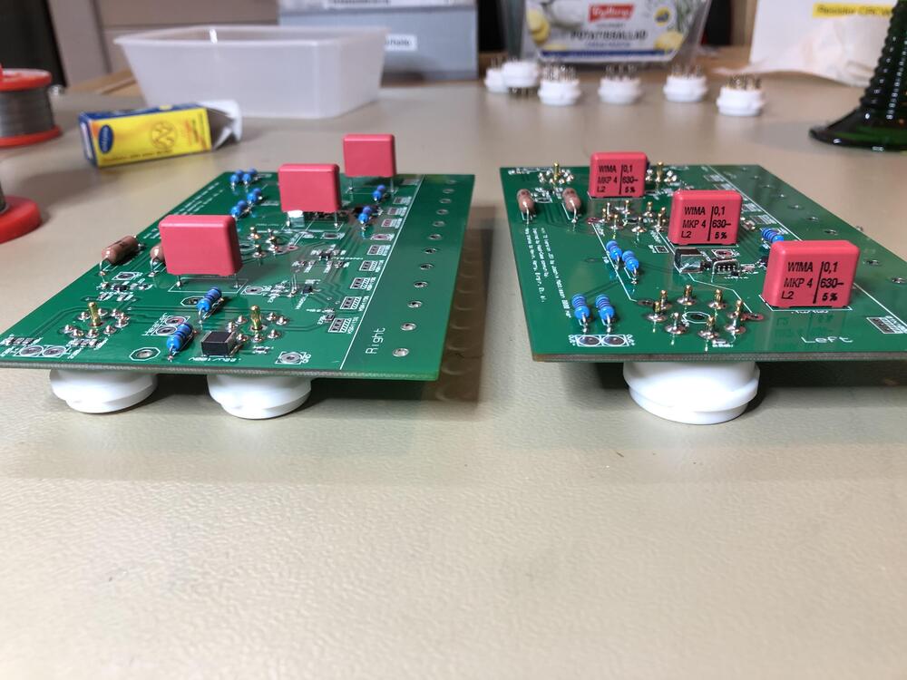 1 point1 pointWhile working with latest mini T2 (version .23) boards today I discovered that op amps on left channel have wrong (old) values. The op amp on none tube side, close to VOL168A, should be OPA197. Op amp on the other side should be LF356. Silkscreen right channel seems to be correct.1 point1 pointMini T2 Switch off thump. I have found that when switching off the mini t2 (golden reference LV and HV supplies) I get a thump on both channels around 3 to 4 seconds after pressing the off switch. I get no thump on switch on using a 45 second delayed HV so I guessed the LV was dropping faster than the HV at switch off. This was confirmed with a multimeter. Compared to the blue hawaii, the mini t2 drains the HV caps at a slower rate but drains the LV caps faster. I solved the switch off thump by replacing the standard 4700uF caps in the Lv supply with 22000uF. This provides significantly longer LV voltage on switch off and stops the thump. I used 30mm diameter Nichicon 22000uF 35V caps which just fit in place of the 50V 4700uF caps. I suspect 15000uF would probably work to. regards and happy mini t2ing1 point1 pointHere is a picture of my third mini T2. Area for heat sink bracket screw holes cut away. Board now 160mm x 80mm and transistors mounted direct to heat sink. Inner dimension of case is 200mm x 161mm. This is the way I’ve built my amplifiers for some years now. There simply is no room for terminal blocks – will only make things more complicated for me. The real thing - DIY T2 has no tblocks either (except for output to Stax connector).
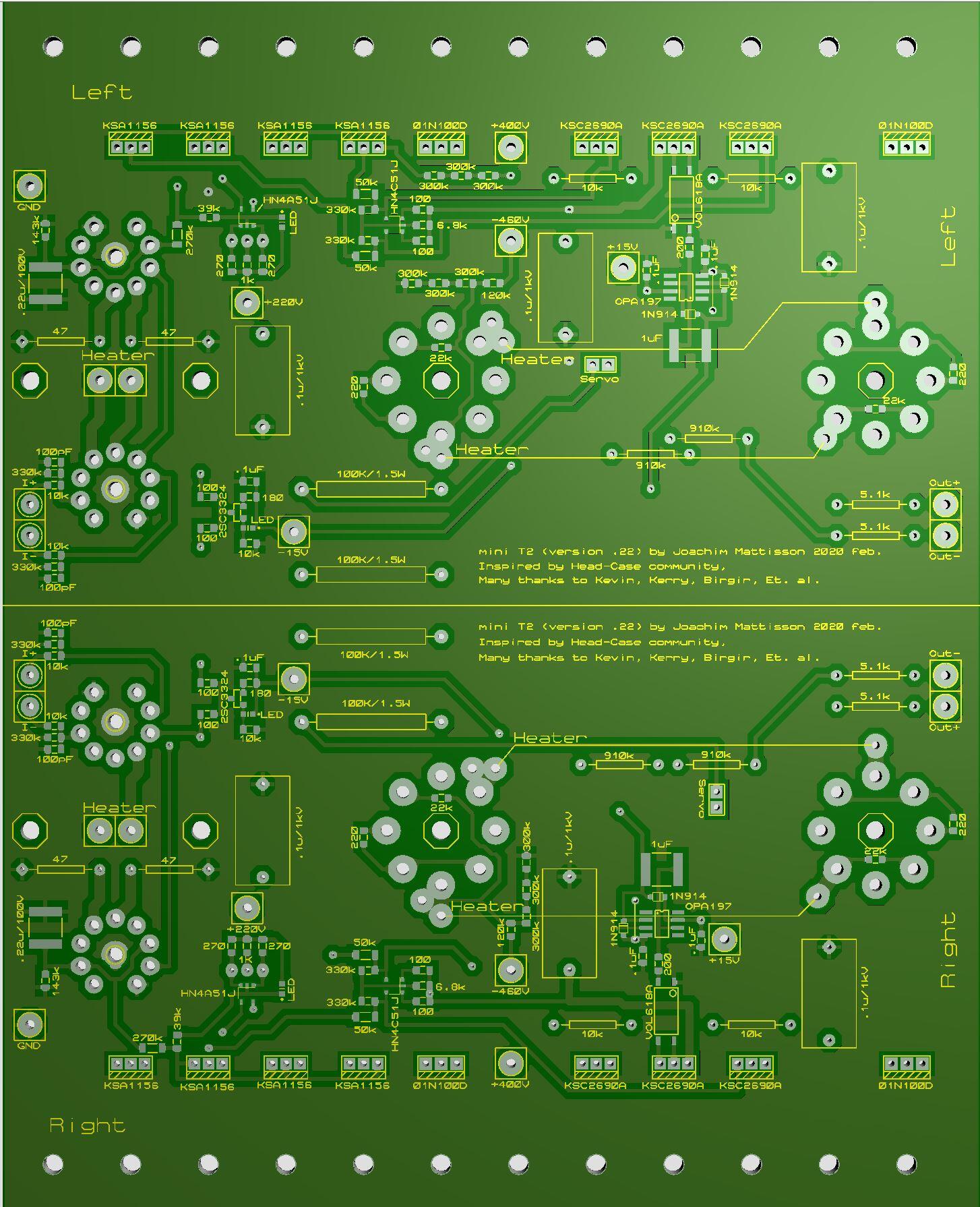
 1 point1 pointIntention is to have updated schematic and BOM at just on place to avoid different versions floating around. This place is the first post of this thread. The advantage is that I, as the disorganized person I’m, cant publish schematic or BOM whenever I feel for it. I need Michaels (mwl168) approval and he is the only one that can make changes public – in the first post of this thread. Anyhow, please take look at the new files for errors or other issues. Below are 3D prints of the new layouts (them I'm authorized to publish myself) Please check for errors. I appreciate feedback especially regarding silkscreen, if anything seems unclear, let me know. Changes: Some resistors value. Offset balance op amp: OPA197, hopefully more reliable. Balance servo op amp: LF356, is more similar to LF353 in the DIY T2. OP27 seems to be reliable in this position though.
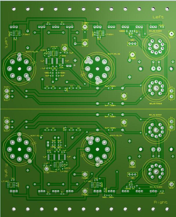
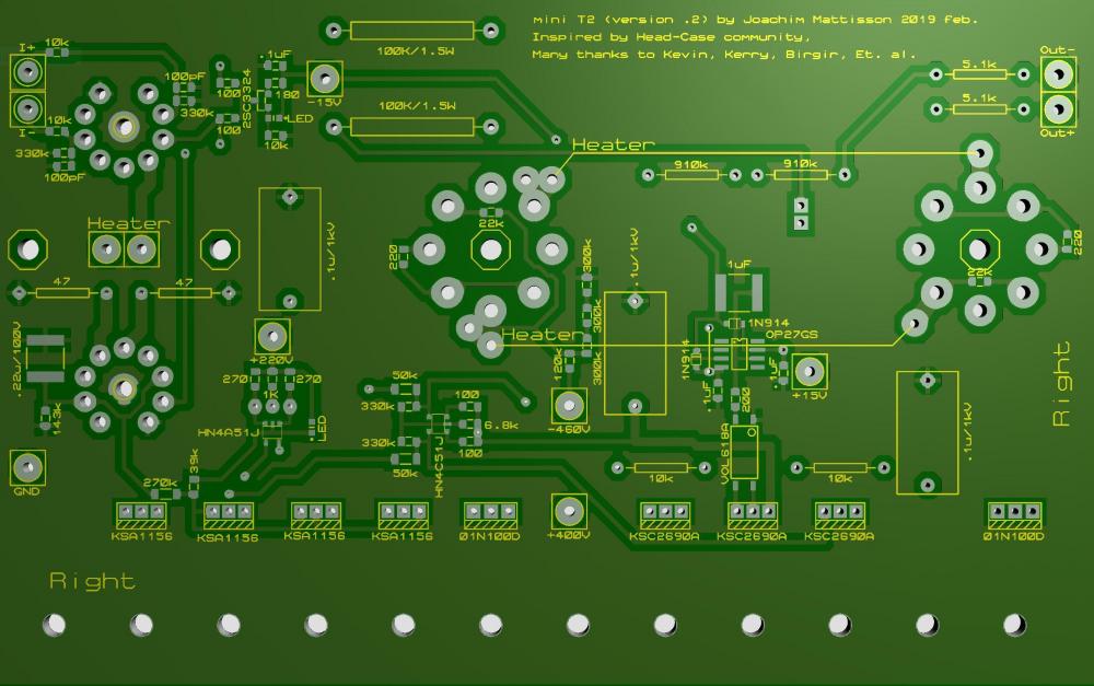
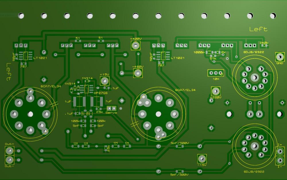
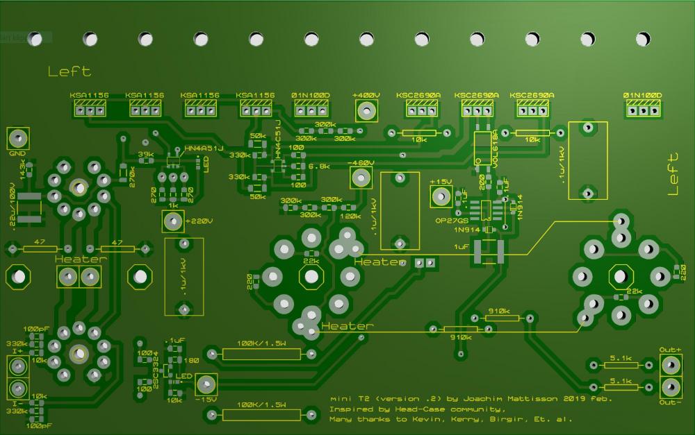
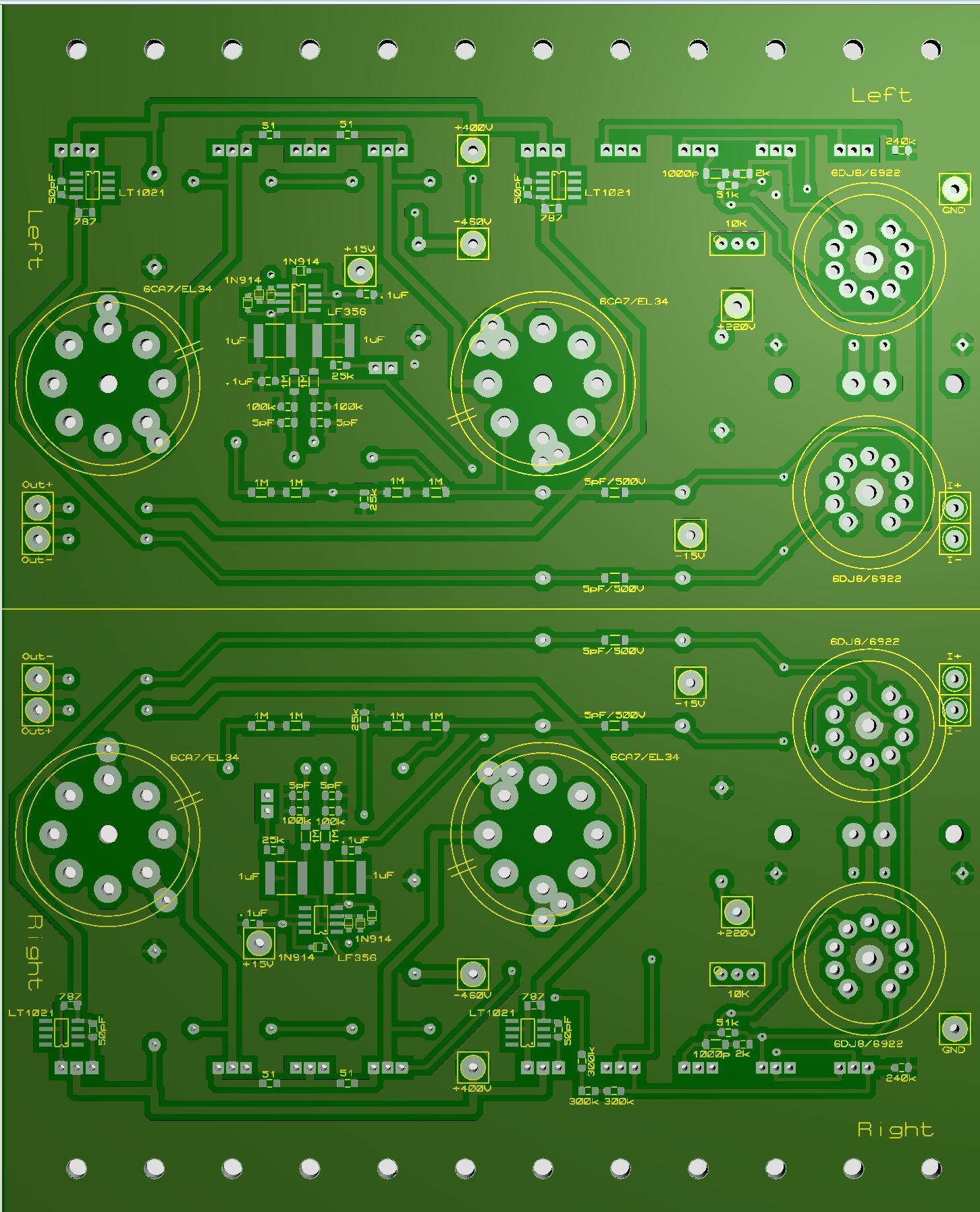
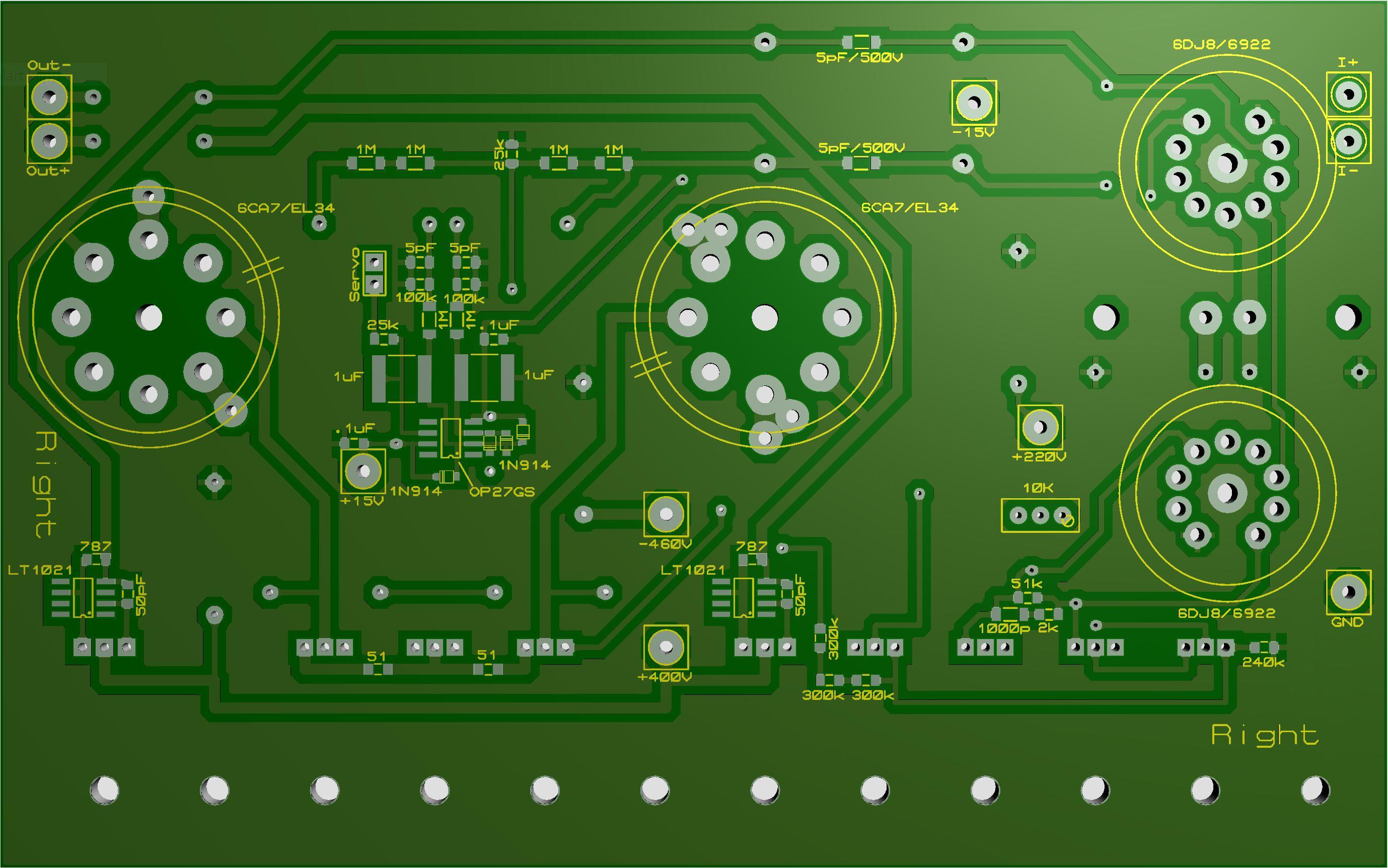
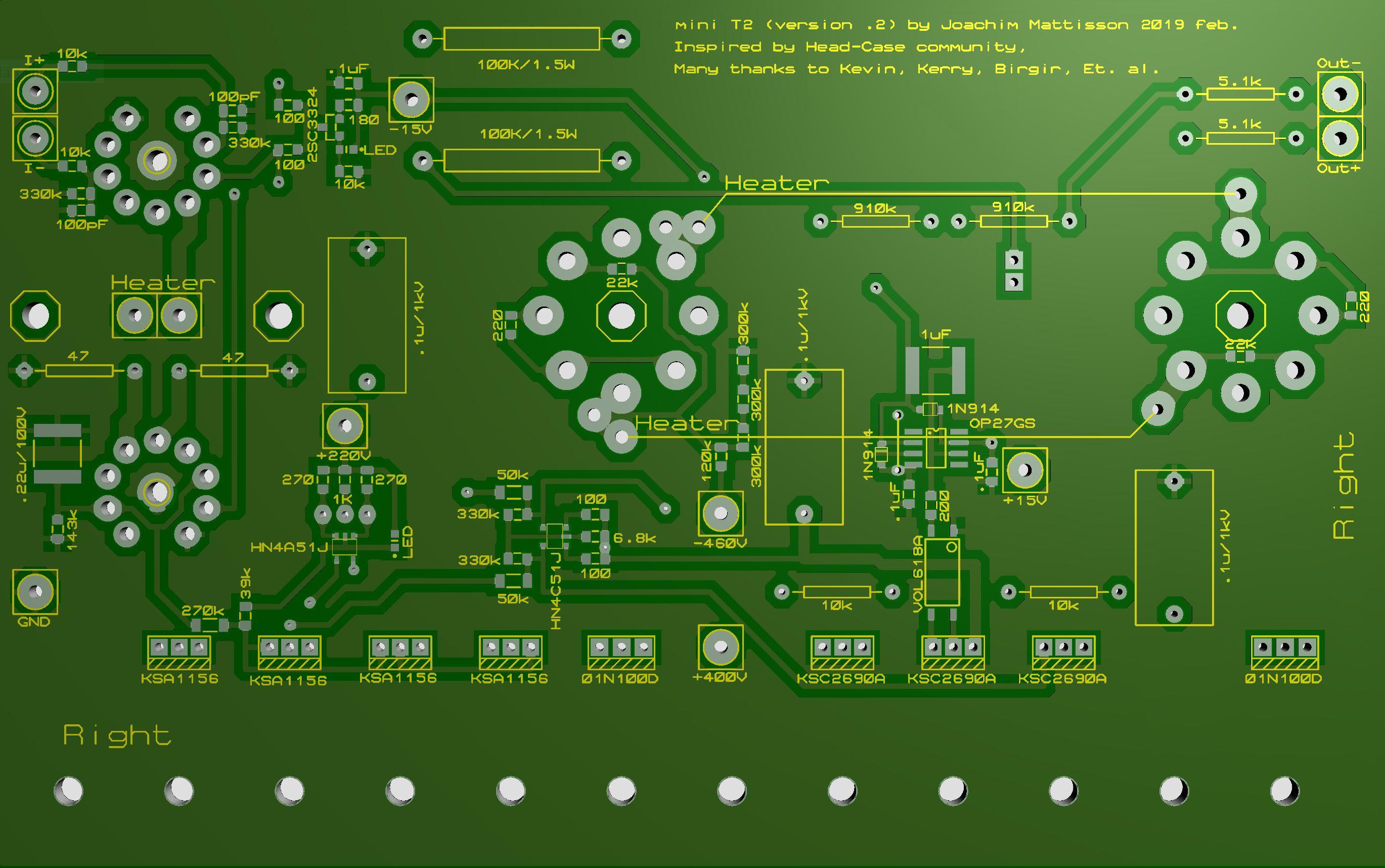
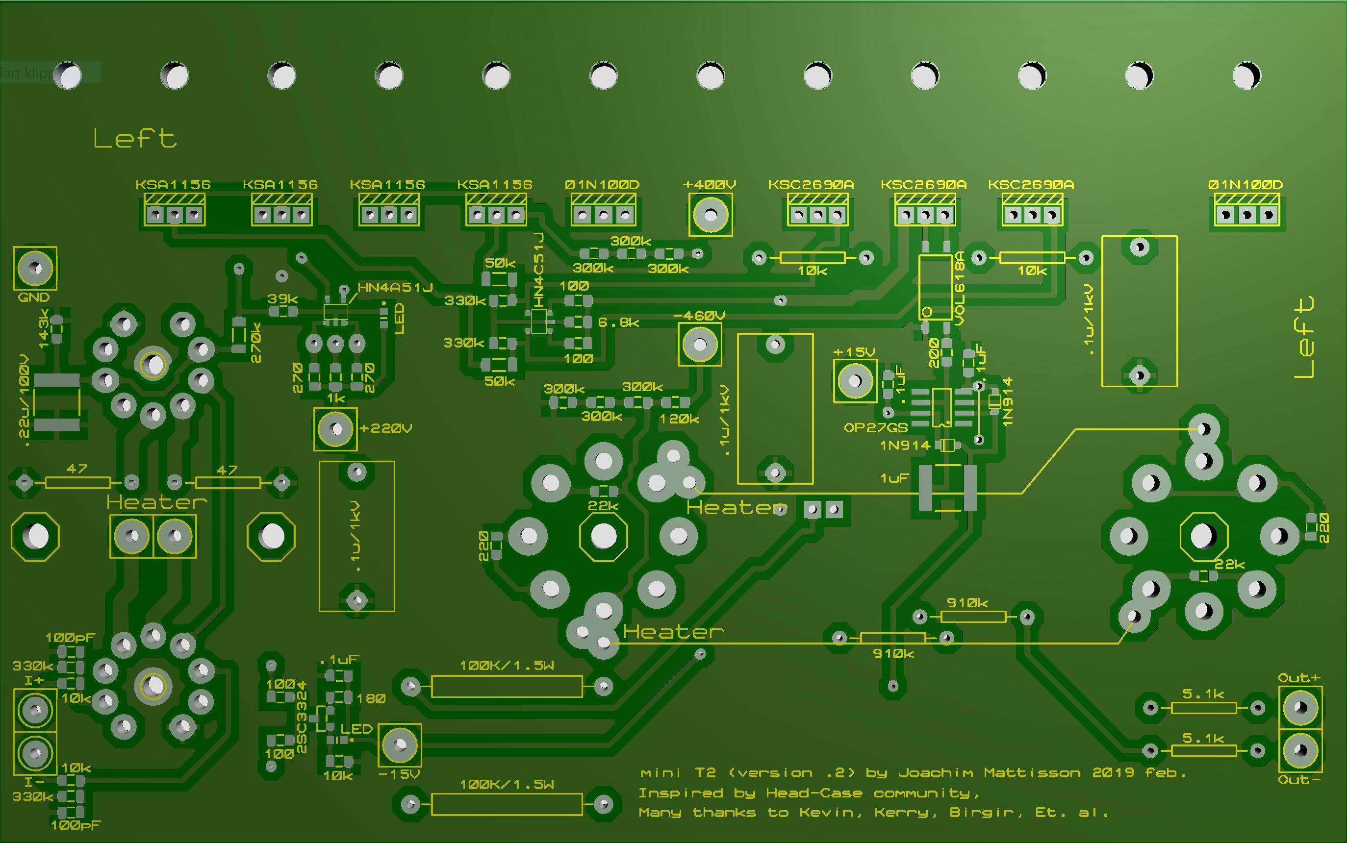
 1 point1 pointA few points regarding the boards Michael have had made on my gerbers. They are basically the same as my kitchen made boards I made five months ago. The small tube footprint has no hole for the center pin. So far I’ve cut away the center pin on the small tube socket after checking the pin holders to be not to tight nor to loose. One time I got tube sockets where the tubes fell out when turning upside down. So either you have to cut pin or drill a hole. Be aware that upper tube has a trace between the grids that might be to close to center pin. Right board 270K resistor has a 0805 pad (intention was 1206). It’s possible to solder a 1206 resistor on the 0805 pad. If +220V you get about 130 V cross the resistor so Vishay CRCW0805 is OK here. But with +250 V you get close to CRCW0805’s limit of 150 V. Some of component values on silk screen are poorly place and almost unreadable. The blame is entirely on me, I’m very sorry. There are four octagons on bottom side. One at each big tube socket center hole and one each side of small tubes filaments connections. Here I have standoffs. A few comments on updated layouts. Small tube footprint with center hole. 270K resistor pad corrected - now 1206. Silk screen remade. Pleas notify me if there is any left that needs additional attention. Now “value” of connections on both sides (except heaters). No terminal blocks on my boards. Top right. Updated 2019-02-27. Bottom right. Updated 2019-02-27. Top left . Updated 2019-02-27. Bottom left. Updated 2019-02-27. I call above version .2. My kitchen made and Michaels are version .1. Regarding this amplifier - there is nothing I've invented. I just have picked up different things and tried to put them together. As: Opto servo (the only offset servo you need) by Kevin. 01N100D/TL1021 current source by Kerry. Schematic of Stax T2 provided by Kevin, Et. al. Schematic of Stax T8000 provided by Kevin and Birgir. Etc. etc. Thanks for all knowledge, information and inspiration from you DIYers and Head-Case members. Please look for errors or other issues.
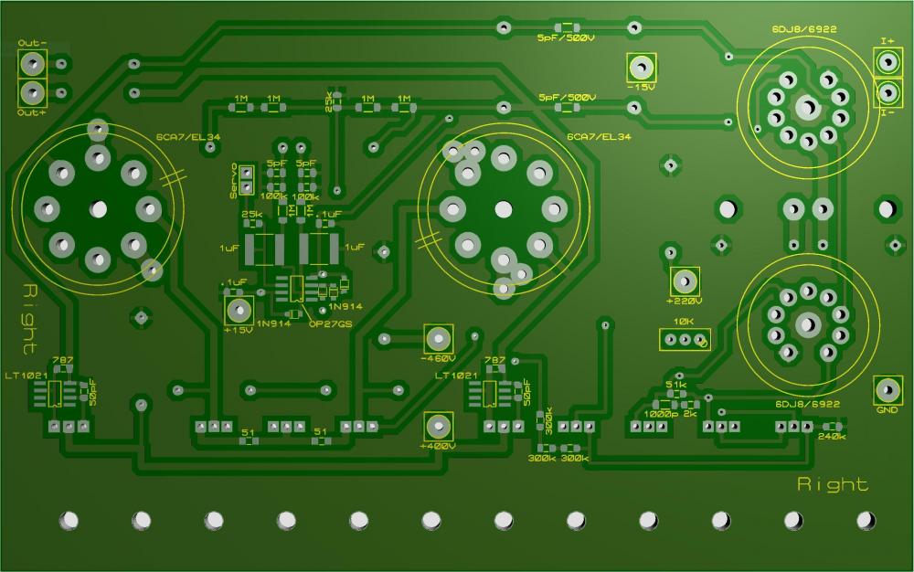
 1 point1 pointOK – Connected an unmodified T2 PSU. Raised voltages to +250 and +/-500V. Top 6922 anode voltage sits at 227V and grid at 78V. So far it works. Will run this for a while and check for darkening spots on the boards.1 point0 points0 pointsRIP to a random person: Krysten Gentile. Krysten died a few days ago, at age 40, of stage 4 metastatic breast cancer. She worked at the same company as my wife Karen; I was able to meet her once when she and Karen had a Zoom call with each other. I poked in and had a brief but very pleasant chat; Krysten's persona - so bright and beautiful - shown through even in that brief moment. A truly beautiful and amazing woman, she fought hard, and was public in her fight and in positive thinking to help others. She created a web site & podcasts with another Philadelphia-area woman with stage 4, "Making The Breast Of It." She touched Karen's life, and even a tiny bit of mine. Obituary: Krysten M. Gentile (nolanfidale.com) And....FUCK cancer!0 points0 points


Important Information
By using this site, you agree to our Terms of Use.