

Leaderboard




Popular Content
Showing content with the highest reputation on 12/03/16 in all areas
-
3 points
-
2 pointsI've never been to NYC before seems like this could be a good reason for a first visit...2 points
-
2 points
-
2 points
-
Here's a great video to help put you guys in the holiday spirit! Enjoy and Happy Holidays from ironbut!2 points
-
2 pointsFrench to Ottoman! Wow - I had no idea that Ottoman was a language. Could have been worse. In the late 1800's a genius called Pedro Carolino produced a phrase book for Portugese tourists visiting Britain. He did not know any English or French, but he did have a Portugese-French and a French-English dictionary. So he generated a phrasebook of originality and beauty, hauling Portugese into English through two languages unknown to him. Who can guess at what "To Craunch a Mormoset" could possibly mean. English as She is Spoke http://www.gutenberg.org/ebooks/304112 points
-
2 points
-
2 pointsRIP good buddy... This past may I lost the last of 5 cats that I had kept together from birth to death since 1997. I had him for 19 years! Longer than my kids have been alive. It's a gut shot indeed2 points
-
1 point
-
I've been playing the 3 disc set nonstop this week. I think it's better than everything since the early nineties. Better than load, and everything after. It's really good car drive music. The Dio medley is really nice. I didn't realize how much I missed this. They were my favorite band in middle school through high school. /wipes tears1 point
-
In. Good people and good causes deserve support, no matter they're overseas1 point
-
There are few kinks on the page. I have requested the point out more clearly what the winner gets. It's at the very bottom and not clear. I also asked them to make sure they have a way to assign a ticket number for each one purchased. I'm hoping to have this worked out today. As most of you know, this is especially important for me because of my son. He is, hopefully, a couple of months away from graduating from SOF combat medic school and will have at least another year before he is deployed and he will be deployed. We lost 6 SF soldiers in a matter of a few days last month, most on deployment and one in training down in Key West. When you hear boots on the ground in Iraq, Syria, Afghanistan, it is likely an SF soldier and/or other SOF soldiers, sailors, marines and airmen. The GBF is a good organization which sometimes is as silent as the soldiers they serve which means not many even know it exists. So, thanks in advance for helping!1 point
-
1 pointThay would be in severe contravention of my unbiased and amateur status.... Becoming a professional reviewer would counter and negate any vestiges of veracity and factual reporting I may have ever possessed or had thought to have acquired in my long and tumultuous journey in the realm of high fidelity and the acquisition thereof.....1 point
-
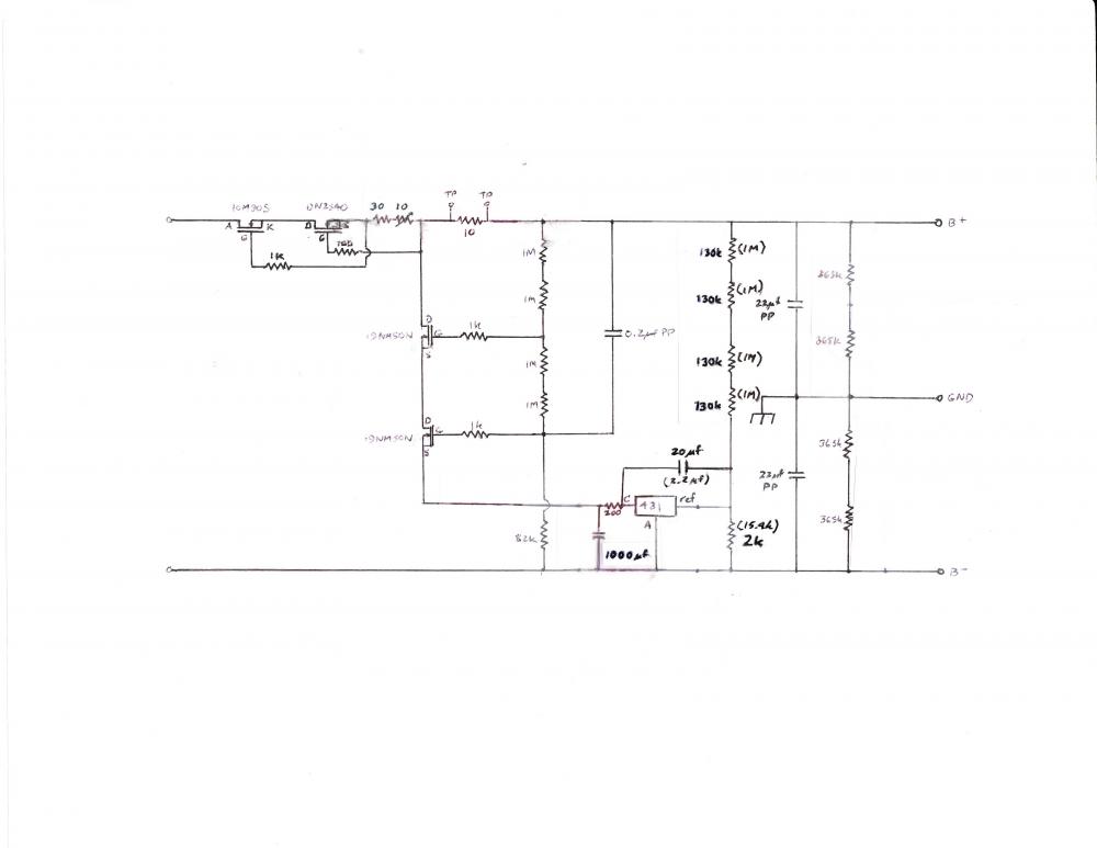
1 pointI've posted a revised power supply schematic and explanation on the SRX revised thread. This comes as a result of trying to make the supply quieter. Most of my attempts seemed to make it noisier, but after frying a few 431 chips, including getting some hundred plus volt oscillations, this is both quieter and more stable.1 point
-
1 pointI have made a few revisions to improve the power supply – see schematic. First, the 15 volt zener at the bottom of the two MOSFET cascode shunt was deleted as unnecessary. Second, the 431 output filter capacitance was increased to 1000 μf to roll off its output noise above 0.8 Hz. Third, I now recommend running a 220 kilohm resistor from B- to each input tail current source, so I deleted the –C supply resistor chain. Fourth, I recommend floating both filament supplies rather than tying them to the high voltage supply, so I modified the voltage setting output resistors to all have the same value. Fifth I decreased the resistor chain values for the 431 chip the schematic shows the original values in parentheses. These are mostly deletions or changes in values but not in topology, i.e. if you leave out the component values the circuit looks pretty much the same as the original. Finally, I moved the capacitor from between reference and anode terminals of the 431 to across its cathode and reference terminals. Although this appears to be a very simple change, it significantly improved both stability and noise performance. The 431 has an internal op amp with a gain of about 55 dB and a bandwidth extending to between 5 kHz to 50 kHz before rolling off. This op amp is not unity gain stable, which means it can and will oscillate. Despite this, the 431 chip is widely used as a voltage regulator in switch mode power supplies in all sorts of consumer electronics, such as PCs, laptop chargers, cell phone chargers, solar panel charge controllers, etc., so various techniques have been developed to stabilize it. The regulator voltage is controlled by feeding back a portion of the output voltage into the reference terminal of the 431. Often a wide bandwidth is desirable to control both the DC voltage and cancel any AC variations across a broad spectrum. However, this design uses local feedback to the lower MOSFET via a capacitor to its gate to cancel any AC changes and noise, so we want to restrict the 431 to controlling the DC only. Broskie did this by rolling off the feedback signal using the capacitor between reference terminal and ground. But that did not affect the feedback loop gain, leaving lots of opportunities for oscillation. However, instead of limiting the feedback signal, if we limit the bandwidth of the 431 sufficiently, we both restrict its effect on AC voltage variations and stabilize it against oscillation. This is done by removing the capacitor between the 431 reference and anode terminals, and instead connecting it between the 431 cathode and reference terminals. In combination with the resistor chain between B+ and the reference terminal, this forms a negative feedback compensation loop that rolls off the gain of the op amp at 6 db/octave above its corner frequency. Since I modified the 431 resistor chain and output RC filter, I used trial and error to determine the needed feedback cap value. There were large oscillations with a 1 μf cap, while 3.3 μf produced smaller, slower oscillations but still managed to fry the 431. A 10 μf/50V polyester capacitor was stable with generally low noise, but random bursts of higher noise – however, the levels of the bursts were still below the 2 mV noise level in the original design. Increasing to 20 μf decreased the magnitude and frequency of the random noise bursts by about half. With the original 4 megohm resistor chain for the 431, a 2.2 μf cap should give the same gain compensation curve, so the simplest modification is to remove it from its original position across the reference and anode terminals and connect it between reference and cathode terminals. On the PS PCB there isn’t room to mount a 2.2 μf cap next to the regulator chip but you can drill a couple holes next to the 200 ohm resistor on the opposite side from the 22 μf output cap and run insulated wires to the two outer leads of the 431 chip. Note that if you are using a polarized cap, the + terminal should be connected to the cathode and the - terminal to the reference. This is the opposite from the previous connection where the + terminal of the cap was connected to the reference terminal. Replacing the TL431 with the quieter SPX431 dropped the noise voltage another 10 dB or so. With these changes, the broad-band power supply noise with a Fluke 189 DMM was decreased to around 0.16 mV into a resistor dummy load on the kitchen counter, with occasional bursts up 0.4-0.5 mV, so call it a -120 dB power supply. Not too shabby considering its simplicity. DC voltage overshoots by a volt or so but then remains within 0.1 volts of its target voltage due to the excellent temperature compensation in the 431 chip.
 1 point
 -
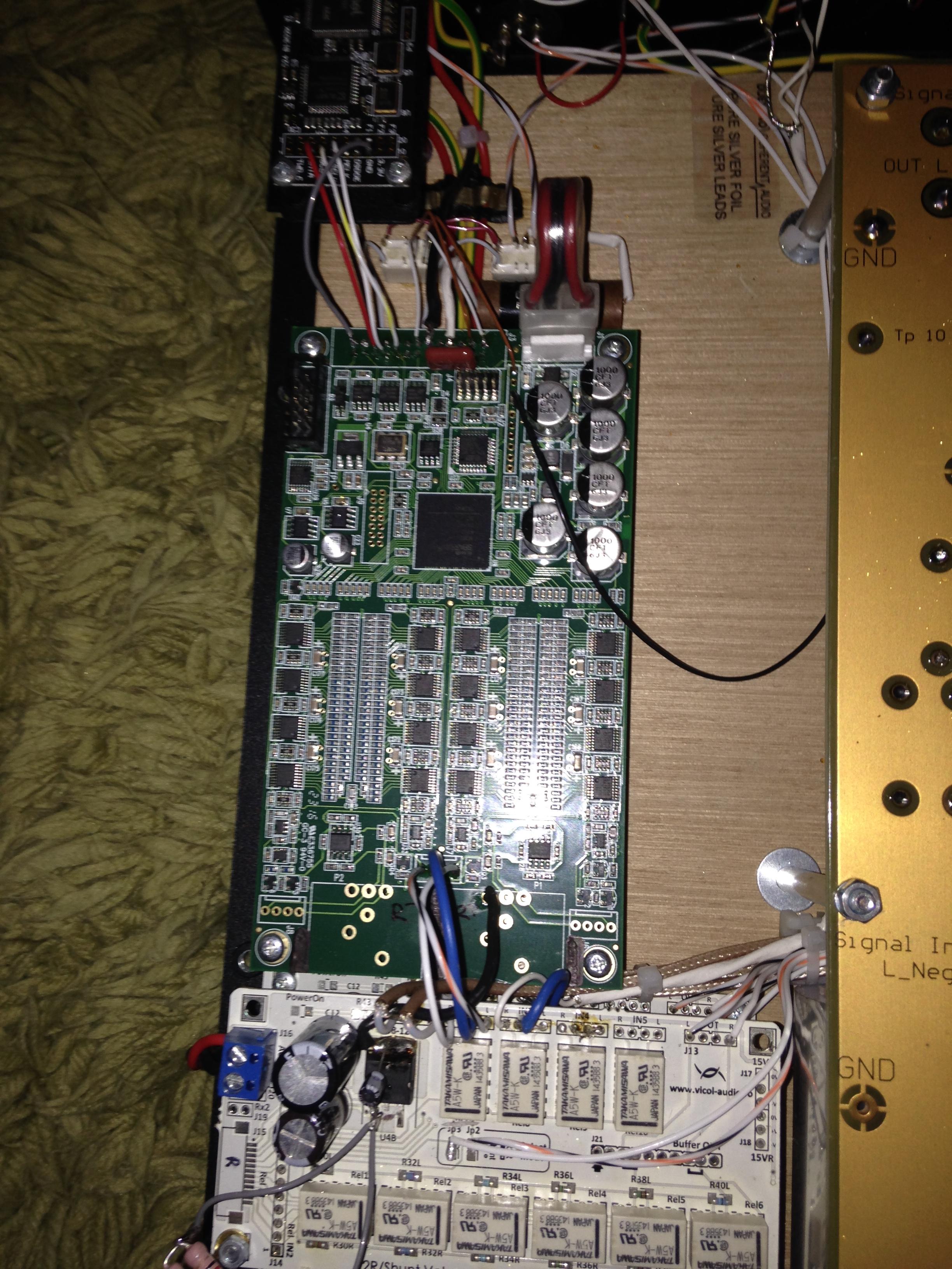
1 pointTest Tone @ Home live right now: http://mixlr.com/illuminator/chat1 pointWe'll meet with Mr. Tyler, Sir. I got a dac based on AD 1862; MHDT Lab Atlantis. I guess, when the time comes we'll compare them properly.1 pointI haven't looked into this at all, so could someone describe how these discrete designs compare to the old ladder chips (PCM63, 1704, et al.)? People like Audio-gd somehow got their hands on new old stock and are still making stuff with them, and most of HC probably still have an old DAC or two that use these R2R chips.1 point1 point1 pointBut, but, this is the bleeding edge of "state of the art" technology where mere mortals just don't understand the synergy involved in the creation of this technological and artistic combination which transcends the mere composition of the individual elements and propels it up to stratospheric heights whereupon it gathers momentum on it's downward trajectory with the aid of gravity to once again transmutate into a melange of ill fitting and contrary juxtapositions of it's components as it attempts to occupy the same space as the hard ground as it comes into contact with the same thus forever altering it's configuration and even surpassing the meagre and mediocre parameters of it's design and acheiving true artisan status worthy of display in any establishment of the finer arts, and moreso, perhaps being worthy of the ultimate accolade which could be garnered by such a contraption, that being a ceremonial procession by a suitable vehicle for this journey, a dumpster, to it's permanent home at a local tip where the local denizens do heap voluminous offerings of their refuse and undesirable matter to venerate the presence of this worthy recipient of their homage.1 point1 pointI just attached these as the world has to see this garbage. The list price is 19000$ plus the dac's which are 2000$. Yup...2k$ for two ~200$ modules. A few highlights for me are the mains transformer glued upside down into the wood with exposed mains wiring. Other parts glued into the bottom plate and almost no connectors used anywhere. I really think that is the best sign of a hack, shit is just tacked together with no care and they hope for the best. I think we have a new Single Power on our hands or Mikhail moved to Poland.
.thumb.jpeg.b228406f5b48728d001ef759c0f776b7.jpeg)
 1 point1 pointI may be going out on a limb here, but I think we should leaf this alone as it is a case of barking up the wrong tree, as the root of the problem is to be found in another branch of the hyperbole surrounding this general topic. if you are inclined to bore into it, you will get to the heart of the matter in which many pithy statements are to be unearthed, and other facts that may stump you.1 point1 pointhttps://world.taobao.com/item/525195615222.htm?fromSite=main&spm=a312a.7700824.w4004-12659368213.2.4SmcUz another discrete R2R module for you guys to play with.1 pointThe fires in Tennessee are so intense, they melted the aluminium on this car. Falls Creek Falls, WA Lake Moraine. Showgirls play chess between shows at New York's Latin Quarter nightclub, 1958, by Gordon Parks. Christmas Market in the Germany's Black Forest. Mount Rainier, with Mount Adams in the background. Medina River, TX. Ozark Mountains of Arkansas. The view from Neuschwanstein Castle, Germany. Kilauea, Hawaii, USA Southern tip of the Baja. Green River Lakes, Wind Rivers, Wyoming, USA. Campfire at Beaver Park, Wind Rivers, Wyoming, USA. Rocky Mountains. Mt. Hood's north side. Nā Pali Coast, Kaua'i, USA. The Yellowstone Plains.1 pointBurial - "Young Death"/"Nightmarket" https://burial.bandcamp.com/album/young-death-nightmarket-hdb100 Yup, this is win.1 point1 pointFinished The End of Death today. All 3 were excellent. Good stories with believable science.1 point1 pointMarquis de Sade - Tanrıya Karşı Söylev (I dont know book's original name or in English, Maybe "Speech Against God"), Collection of his notes. It's the only book which does not include eroticism I guess.1 point1 pointhttps://en.wikipedia.org/wiki/The_Three-Body_Problem The Three Body Problem by Liu Cixin Fantastic story, and unusual because it's current-ish hard science fiction.1 point


















.jpeg.0a50d80e015b69d5970443e1c73cbf36.jpeg)



Important Information
By using this site, you agree to our Terms of Use.